Semiconductor device having a first circuit block isolating a plurality of circuit blocks

a technology of circuit blocks and semiconductor devices, applied in the direction of semiconductor devices, electrical devices, transistors, etc., can solve the problems of increasing packaging area and cost, reducing the reliability of semiconductor devices, etc., and achieves the effect of suppressing the interference caused by the noise between circuit blocks, suppressing the noise of crosstalk, and high tolerance against crosstalk nois

Inactive Publication Date: 2011-03-15
SEIKO EPSON CORP
View PDF13 Cites 108 Cited by
  • Summary
  • Abstract
  • Description
  • Claims
  • Application Information

AI Technical Summary

Benefits of technology

[0007]An advantage of the invention is to provide a semiconductor device combining a bulk structure with an SOI structure on the same substrate, while suppressing the interference caused by the noise between circuit blocks.
[0008]According to a first aspect of the invention, a semiconductor device includes: a semiconductor layer, arranged, via an insulation layer, on a region of a part of a semiconductor substrate; a first circuit block formed on the semiconductor layer; and a second and a third circuit blocks formed on the semiconductor substrate, isolated from each other by the first circuit block.
[0009]Consequently, a plurality of circuit blocks having the bulk structures can be combined on the same semiconductor substrate, isolated from each other by the SOI structure that has a high tolerance against crosstalk noises. This allows a decreasing of the distances between the adjacent circuit blocks, while suppressing the crosstalk noise between the circuit blocks, thereby suppressing the increase in the chip size, allowing to mount various functional components onto a single chip, while improving the characteristics and reliability of semiconductor devices.
[0010]It is desirable, in the semiconductor device according to the first aspect of the invention, that the first circuit block be arranged between the second circuit block and the third circuit block.
[0011]Consequently, a plurality of circuit blocks having the bulk structures can be combined on the same semiconductor substrate, isolated from each other by the SOI structure, thereby allowing a suppressing of the increase in the chip size, while also suppressing the crosstalk noise between the circuit blocks. Moreover, the periphery of the first circuit block can be surrounded by the semiconductor substrate, improving the heat dissipation from the first circuit block, and thereby improving the temperature characteristic of the first circuit block.
[0012]It is desirable, in the semiconductor device according to the first aspect of the invention, that either the second or the third circuit block be arranged to contact at least one side of the first circuit block.

Problems solved by technology

However, in the case of combining the bulk structure and the SOI structure on the same substrate, an interference caused by the substrate noise may occur between the circuit blocks, depending on the arrangement thereof, resulting in a problem that the reliability declines in the semiconductor device.
On the other hand, if the sufficient distance is provided between the adjacent circuit blocks, so as to reduce the interference caused by the noise between the circuit blocks, then the chip size increases, resulting in a problem of causing an increase in packaging area and cost.

Method used


Image

  • Semiconductor device having a first circuit block isolating a plurality of circuit blocks
  • Semiconductor device having a first circuit block isolating a plurality of circuit blocks
  • Semiconductor device having a first circuit block isolating a plurality of circuit blocks

Examples


first embodiment

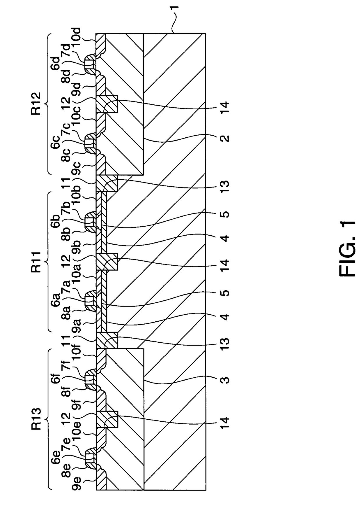
[0056]FIG. 1 is a sectional drawing illustrating a configuration example of a semiconductor device according to the first embodiment.

[0057]In FIG. 1, an SOI forming region R11 and a bulk regions R12 and R13 are provided on a semiconductor substrate 1, and wells 2 and 3 are formed in the bulk regions R12 and R13. Here, the bulk regions R12 and R13 can be arranged on the semiconductor substrate 1 so as to be isolated from each other by the SOI forming region R11. For instance, the SOI forming region R11 can be formed between the bulk region R12 and the bulk region R13. In the case of using a high-resistant substrate with resistivity of more than 500 Ωcm for the semiconductor substrate 1, the substrate resistance under an insulation film 4 in the silicon-on-insulator forming region can be increased.

[0058]In the SOI forming region R11 and the bulk regions R12 and R13, grooves 14 are formed, isolating devices in the SOI forming region R11 as well as in the bulk regions R12 and R13. Moreo...

second embodiment

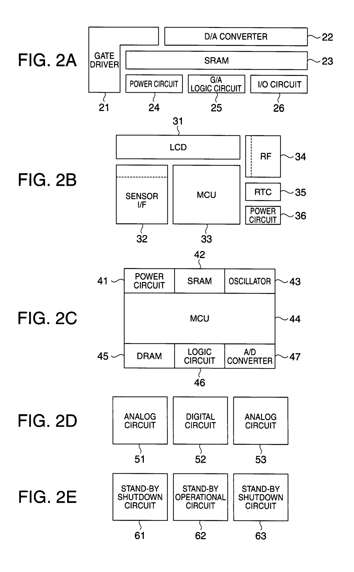
[0066]FIGS. 2A to 2E are top view drawings illustrating configuration examples of a semiconductor device according to a second embodiment.

[0067]As shown in FIG. 2A, a plurality of circuit blocks is mounted on a semiconductor chip, and a gate driver 21, digital-to-analog (hereinafter “D / A”) converter 22, an SRAM 23, a power circuit 24, a gate array logic circuit 25, and an input-output (hereinafter “I / O”) circuit 26 are formed as the circuit blocks. Here, the gate driver 21, the D / A converter 22, the power circuit 24, and the I / O circuit 26 are arranged in the bulk regions, and the SRAM 23 and the gate array logic circuit 25 are arranged in the SOI forming regions. Moreover, the circuit blocks formed in the bulk regions can be arranged to contact at least one side of the circuit blocks formed in the SOI forming regions. Further, the circuit blocks formed in the SOI regions can be arranged between the circuit blocks formed in the bulk forming regions.

[0068]This allows a decreasing of ...

third embodiment

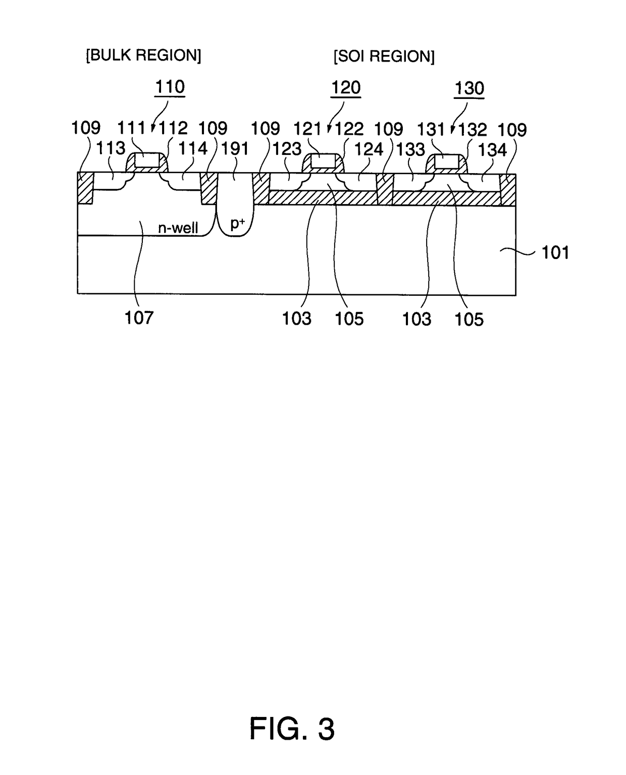
[0076]FIG. 3 is a sectional drawing illustrating a configuration example of a semiconductor device according to a third embodiment.

[0077]As shown in FIG. 3, this semiconductor device has the bulk region and the SOI region formed in a semiconductor substrate 101. Here, the bulk region means that the region has only the semiconductor substrate 101 as an underlying layer. Moreover, the SOI region means that semiconductor layers 105 are formed on the semiconductor substrate 101 via insulation layers 103. Examples of the semiconductor substrate 101 include a p-type silicon (Si) substrate, and examples of the insulation layers 103 include silicon oxide film (SiO2). The semiconductor layers 105 are formed with, for instance, Si. Such semiconductor substrate (device) having the bulk region and the SOI region in the same substrate is formed, for instance, with the SBSI method.

[0078]As shown in FIG. 3, a well 107 of, for instance, an n-type, is formed in the semiconductor substrate 101 within...


PUM


Abstract

A semiconductor device, includes: a semiconductor layer, arranged, via an insulation layer, on a region of a part of a semiconductor substrate; a first circuit block formed on the semiconductor layer; and a second and a third circuit blocks formed on the semiconductor substrate, isolated from each other by the first circuit block.

Description

BACKGROUND[0001]1. Technical Field[0002]The present invention relates to a semiconductor device, particularly to the ones in which bulk structures and silicon-on-insulator (hereafter “SOI”) structures are combined on the same substrate.[0003]2. Related Art[0004]Field-effect transistors formed on SOI substrates have been attracting attention, due to their high level of usability such as easiness in device isolation, latch-up free characteristics, and a small source / drain junction capacitance. Particularly, researches for achieving the operation of the SOI transistors in a fully depleted mode have been very active, since fully depleted SOI transistors allow rapid operations with low-power consumption, and can be driven with low-voltage. A method of forming the SOI transistors at a low cost, by forming SOI layers on bulk substrates, is disclosed as an example of related art. In the method disclosed in the example of related art, Si / SiGe layer is deposited on an Si substrate, and therea...

Claims


Application Information

Patent Timeline
Patent Type & Authority Patents(United States)
IPC IPC(8): H01L29/76
CPCH01L21/76283H01L21/823481H01L21/823878H01L21/84H01L27/1203H01L27/06H01L27/10
Inventor KATO, JURI
Owner SEIKO EPSON CORP
Why Eureka
Try Eureka