

Fabrication process for photovoltaic cell
- Summary
- Abstract
- Description
- Claims
- Application Information
AI Technical Summary
Problems solved by technology
Method used
Image

Examples
Embodiment Construction
[0036]According to the present invention, techniques related to solar energy are provided. In particular, the present invention provides a method and resulting device fabricated from a plurality of photovoltaic regions provided within one or more substrate members. More particularly, the present invention provides a method and resulting device for manufacturing the photovoltaic regions within the substrate member, which is coupled to a plurality of concentrating elements. Merely by way of example, the invention has been applied to solar panels, commonly termed modules, but it would be recognized that the invention has a much broader range of applicability.
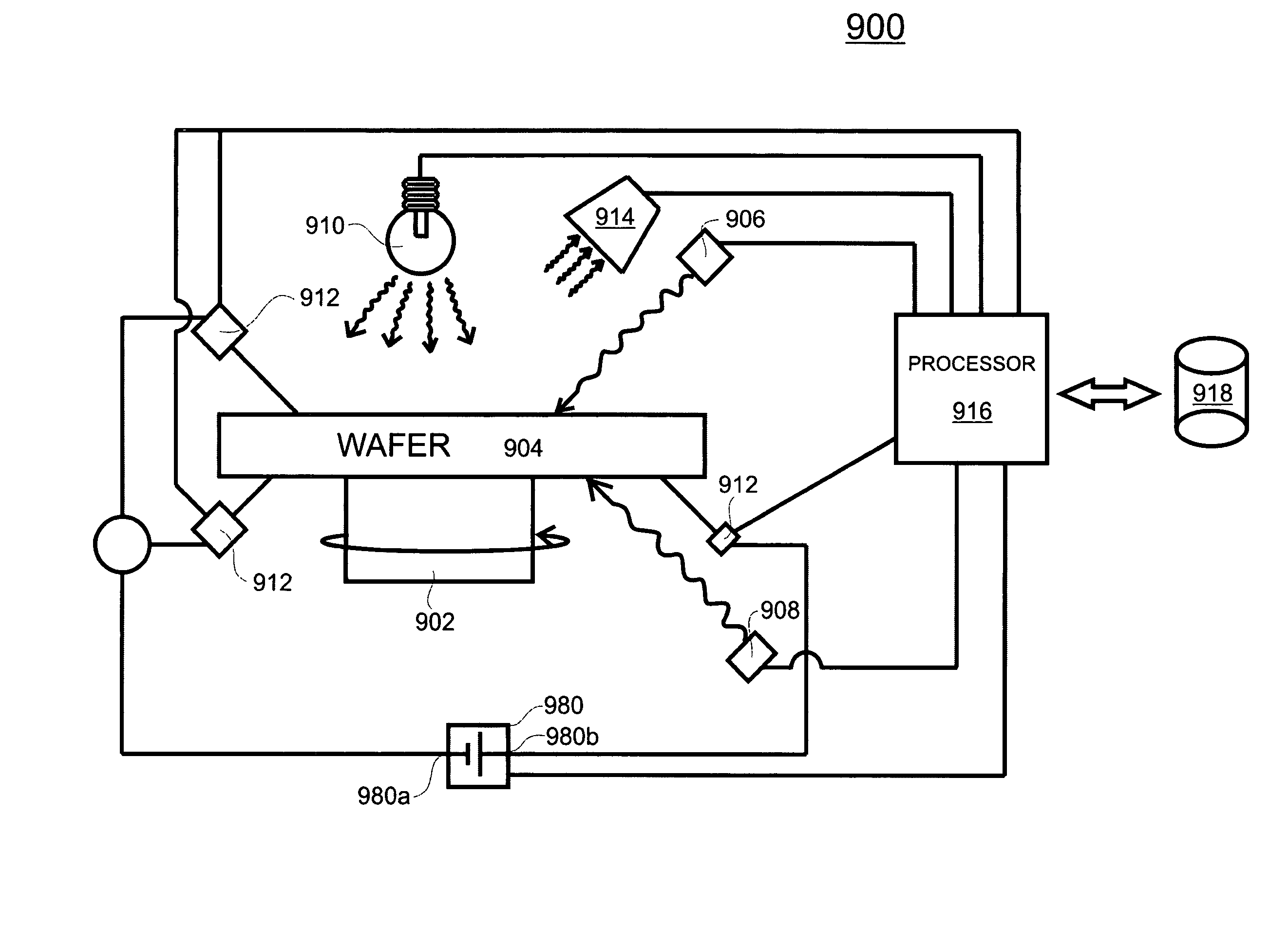
[0037]According to embodiments of the present invention, a photovoltaic strip is physically separated from a semiconductor wafer utilizing physical sawing or other techniques. In accordance with one embodiment, an identity / source of the semiconductor wafer is first determined by interrogating the wafer to identify one or more of it...
PUM
 Abstract
Description
Claims
Application Information