Method of mediating forward voltage drift in a SiC device

a forward voltage drift and sic device technology, applied in the field of forward voltage drift mediating in a sic device, can solve the problems of insufficient recovery rate and inducible recovery, and achieve the effects of reducing the impact of ssfs, minimizing the expansion of ssfs and corresponding vf drift degradation rate and magnitude, and extending the operational life of the devi

Inactive Publication Date: 2011-03-29
THE U S AS REPRESENTED BY THE SEC OF THE NAVY
View PDF1 Cites 2 Cited by
  • Summary
  • Abstract
  • Description
  • Claims
  • Application Information

AI Technical Summary

Benefits of technology

There are several advantages to one or more embodiments of the invention. First, the operation of the devices at elevated temperatures reduces the impact of SSFs upon the devices and minimizes the expansion of the SSFs and the corresponding Vf drift degradation rate and magnitude. This would allow devices that would otherwise be unacceptable for room temperature operation due to high BPD densities to become commercially viable for applications in high ambient temperature environments.
Current-induced induced recovery, the procedure of recovering the Vf drift via SSF contraction under forward bias operation within the above mentioned current and temperature specifications, for example, allows for the regeneration of electrically degraded hexagonal-SiC devices. This enables refurbishment of circuits and / or devices for further use, extending the operational lifetime of the devices, despite some level of SSF-induced electrical degradation having previously occurred. Furthermore, current-induced recovery within a circuit can be induced more readily and often, maintaining the devices within a given voltage tolerance for the turn-on voltage. Current-induced recovery would enable a continued device operation within a circuit without having to be regenerated or replaced for a significantly extended operational lifetime.
In an illustrative embodiment of the invention, the circuitry having a SiC device is exposed to an ambient temperature >150° C. for many applications. Under these conditions, no additional efforts are required, or desired, to cool the SiC devices. When operated, the elevated temperatures would significantly hinder SSF expansion and minimize the Vf drift as well as minimize the impact of the SSFs that did nucleate and expand. When the device is not being forward or reversed biased, a lower, base current could be maintained in the device at this temperature, inducing contraction of any expanded SSFs and recovery of any Vf drift induced. In other words, the device could be operated in TTL-like conditions, where the on-state would be at a given high voltage level desired, and the off-state would be at some lower, but non-zero voltage. Finally, if deemed necessary, the circuit could be temporarily removed and replaced to get a complete regeneration external to the electrical system, after such refurbishment could be reinstalled when necessary.

Problems solved by technology

Smaller currents typically do not provide sufficient recovery rates to be useful, whereas currents in excess of 24 mA / cm2 tend not to induce sufficient recovery to be of use.

Method used


Image

  • Method of mediating forward voltage drift in a SiC device
  • Method of mediating forward voltage drift in a SiC device
  • Method of mediating forward voltage drift in a SiC device

Examples


Embodiment Construction

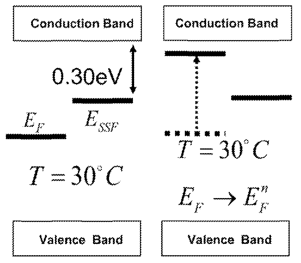
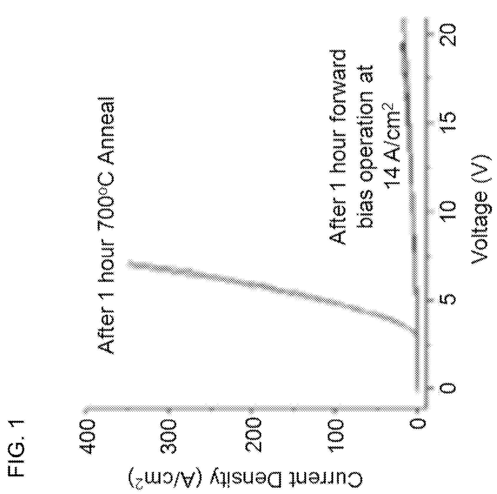
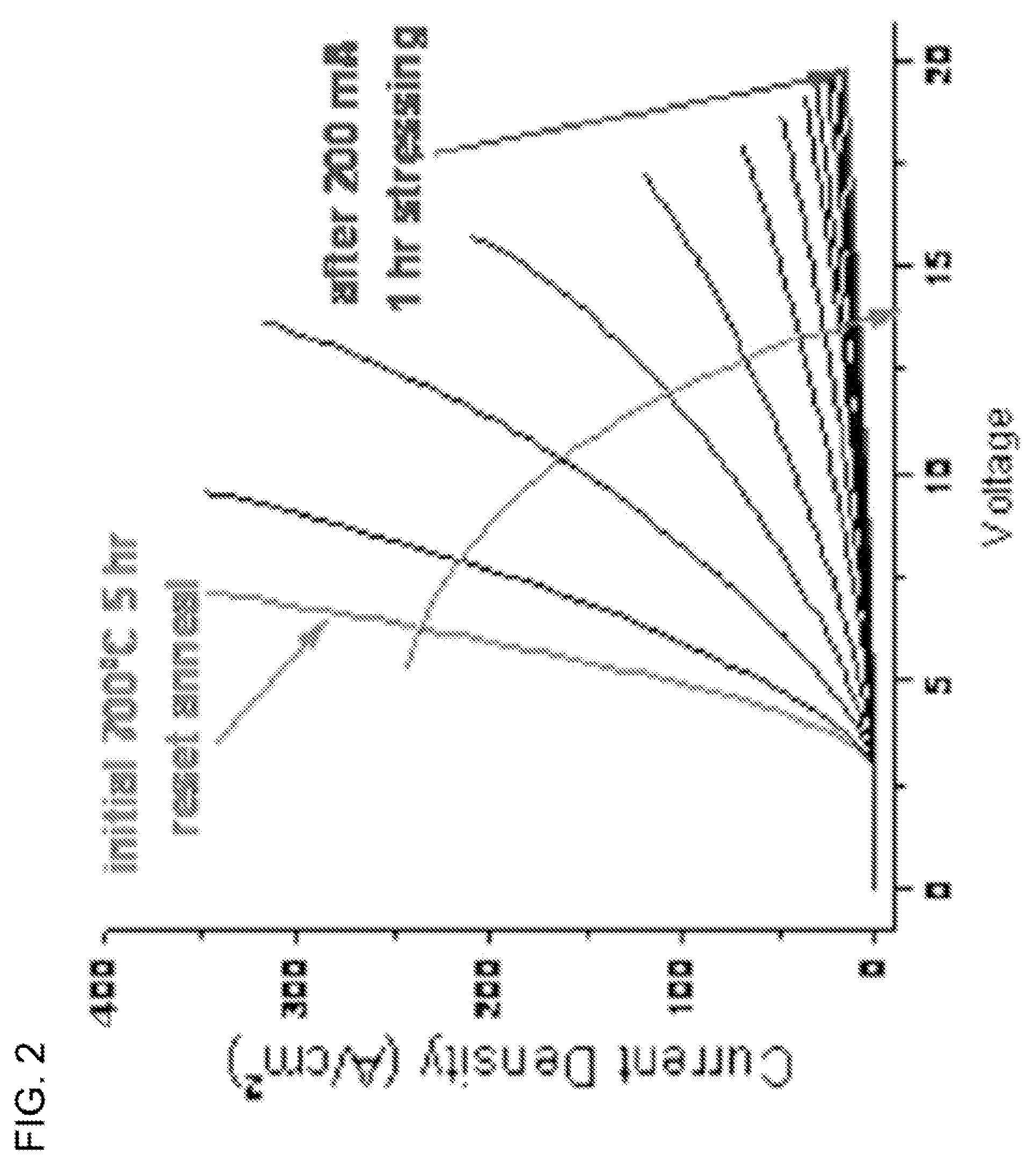
An embodiment of the invention, for example, includes a method of reversing Shockley stacking fault expansion, which in turn leads to a recovery of degradation to the electrical properties of the device (Vf drift, increases in drift layer resistance, reduction in majority carrier conduction current and / or increases in leakage current in reverse blocking mode). The method comprises providing a bipolar or a unipolar SiC device exhibiting a degradation in the electrical properties caused by forward bias bipolar injection that leads to Shockley stacking fault expansion. The SiC device is heated to a temperature above 150° C. and below the maximum operational temperature of the SiC device and packaging. Operation of SiC for recovery procedures is, for example, performed up to temperatures of approximately 700° C., provided that the electrical packaging of the device and contact integrity are not compromised. A forward bias current is passed through the SiC device sufficient to induce at ...


PUM


Abstract

A method of reversing Shockley stacking fault expansion includes providing a bipolar or a unipolar SiC device exhibiting forward voltage drift caused by Shockley stacking fault nucleation and expansion. The SiC device is heated to a temperature above 150° C. A current is passed via forward bias operation through the SiC device sufficient to induce at least a partial recovery of the forward bias drift.

Description

TECHNICAL FIELDThis invention relates generally to a method of mediating forward voltage drift in a SiC device, and, more particularly, to a method of at least partially recovering and / or inhibiting the forward voltage drift that occurs during typical forward bias operation of the SiC device.BACKGROUND ARTSilicon carbide is a desirable material for high power and temperature bipolar and unipolar electronic devices, such as high blocking voltage PIN and Schottky diodes, respectively. Other such devices include, but are not limited to, junction barrier Schottky diodes (“JBS”), merged-PIN-Schottky diodes (“MPS”), double-diffused metal-oxide-semiconductor field effect transistors (“DMOSFETS”), vertical junction field effect transistors (“VJFETs”), bipolar junction transistors (“BJTs”) and insulated-gate bipolar transistors (“IGBTs”). However, the presence of basal plane dislocations (“BPDs”) in the drift layer of bipolar or unipolar devices, where bipolar injection may occur, leads to t...

Claims


Application Information

Patent Timeline
Patent Type & Authority Patents(United States)
IPC IPC(8): H01L21/326H01L21/479
CPCH01L21/0445H01L29/1608H01L29/6606Y10S438/931
Inventor CALDWELL, JOSHUA D.STAHLBUSH, ROBERT EHOBART, KARL DTADJER, MARKO JGLEMBOCKI, OREST J
Owner THE U S AS REPRESENTED BY THE SEC OF THE NAVY
Why Eureka
Try Eureka