System and method for circuit schematic generation

a circuit schematic and system technology, applied in the field of schematic generators, can solve the problems that conventional schematic generators cannot automatically reproduce the functionality, interpretability, and quality as described, and achieve the effect of avoiding the occurrence of errors

Active Publication Date: 2011-03-29
CADENCE DESIGN SYST INC
View PDF6 Cites 197 Cited by
  • Summary
  • Abstract
  • Description
  • Claims
  • Application Information

AI Technical Summary

Problems solved by technology

Conventional schematic generators cannot automatically reproduce the functionality, interpretability, and quality as described above of a hand-drawn analog circuit schematic.

Method used


Image

  • System and method for circuit schematic generation
  • System and method for circuit schematic generation
  • System and method for circuit schematic generation

Examples


Embodiment Construction

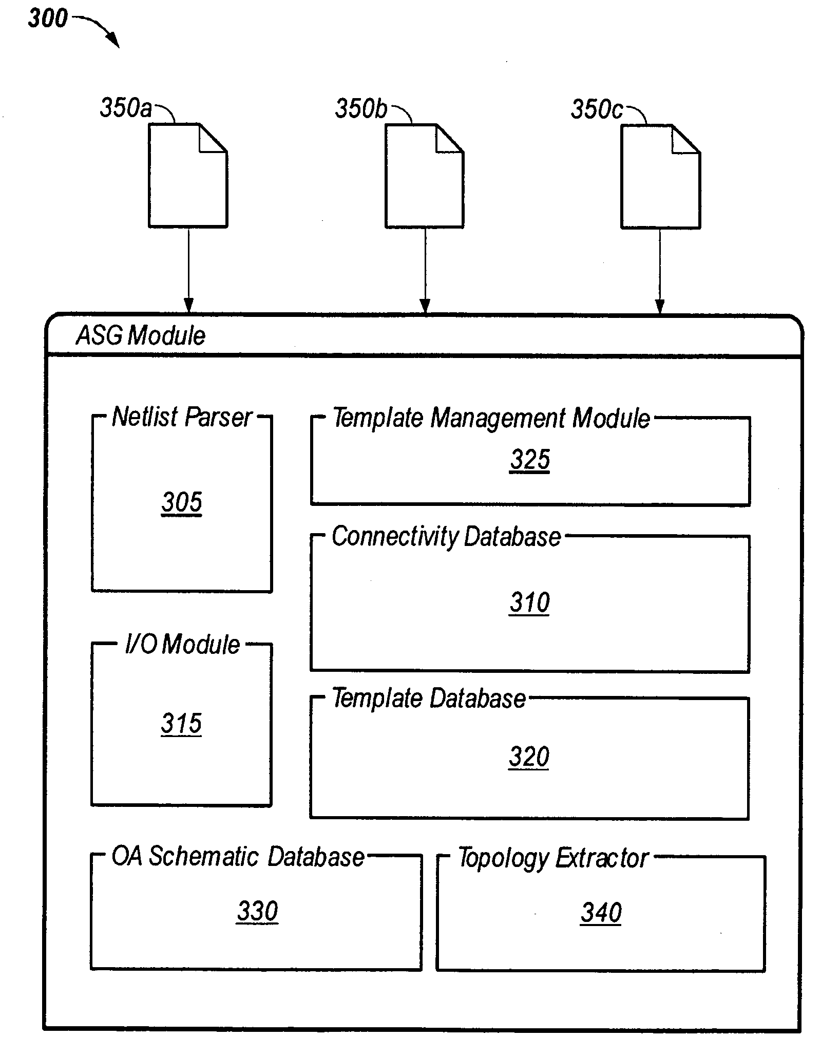
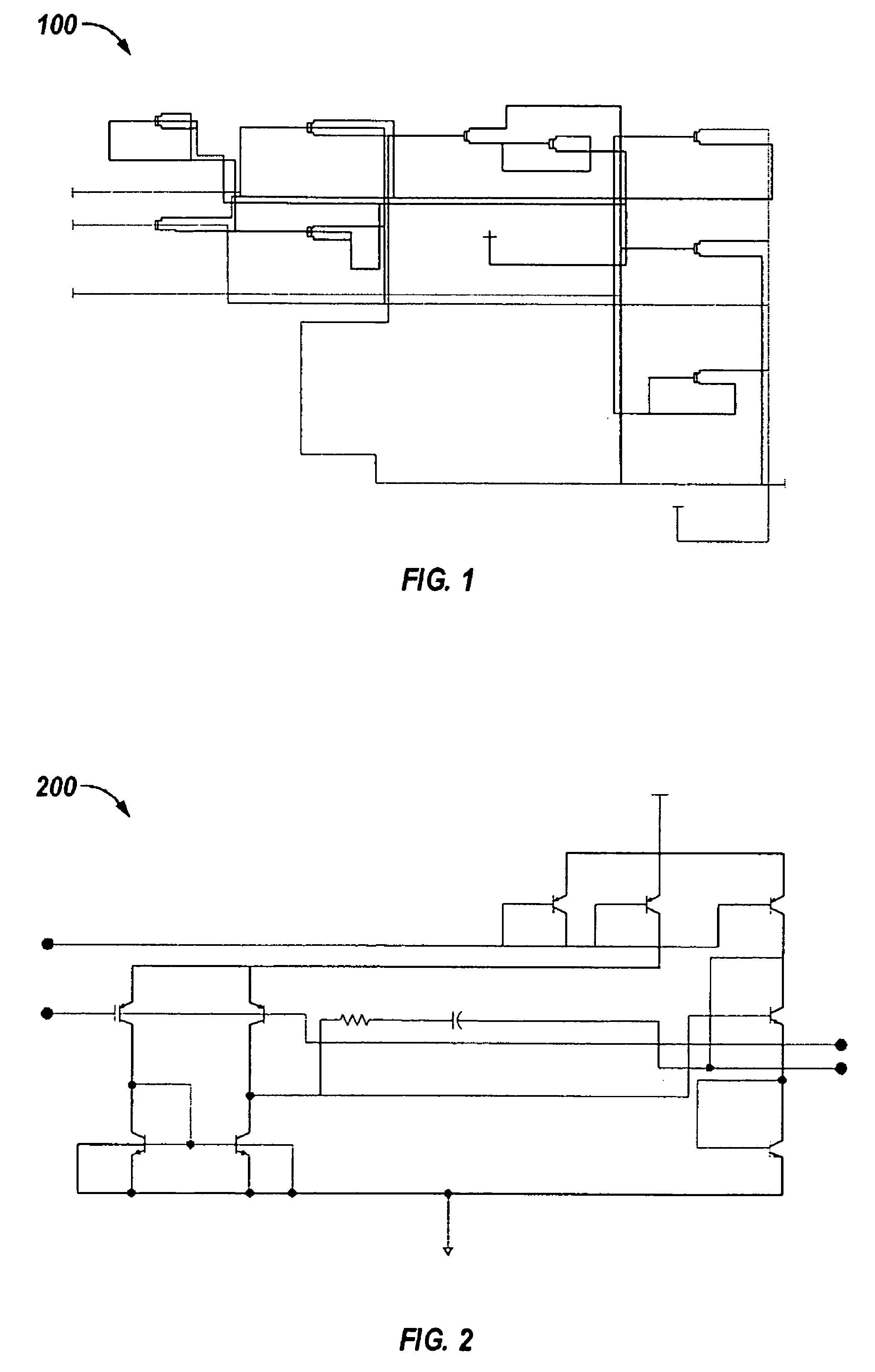
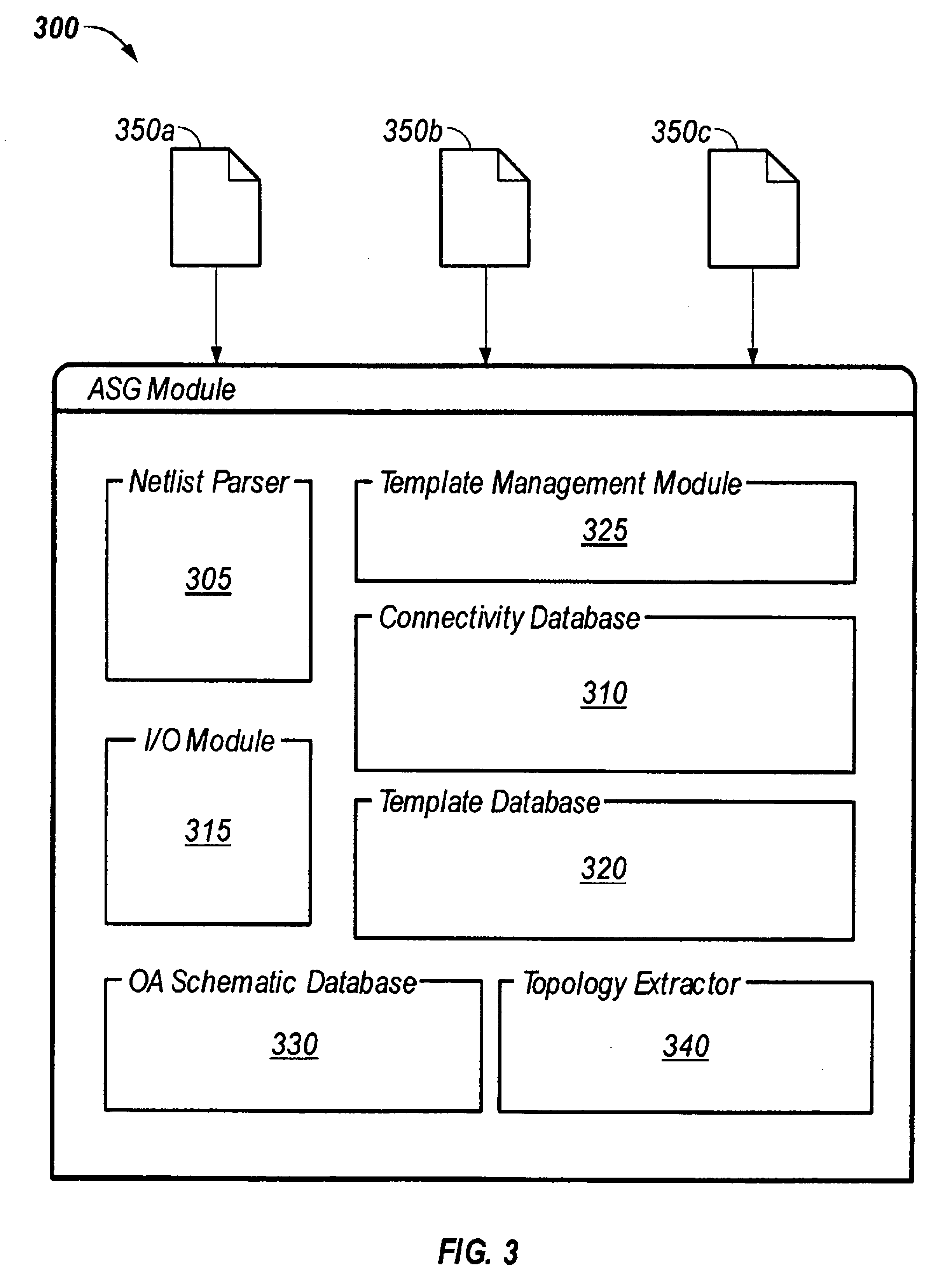
[0003]According to various embodiments of the invention, systems and methods for generating a circuit schematic are provided. In accordance with one embodiment of the invention, a method for generating a circuit schematic includes: identifying a first group instances that match a circuit template among groups of devices; defining placement and constraint data for instances of the first group; creating a circuit schematic having a grid by placing instances of the first group in a column of the grid based on the placement and constraint data; assigning a row to instances of the first group within the grid based on the placement and constraint data; and routing the instances of the first group using the placement and constraint data.

[0004]In an embodiment, the first group of instances comprises n-type MOSFET transistor device (NMOS), a p-type MOSFET transistor device (PMOS), a NPN Bipolar transistor device (NTX), and a PNP Bipolar transistor device (PTX).

[0005]In an embodiment, the def...


PUM


Abstract

The present invention provides a system and method for generating circuit schematic that includes extracting connectivity data of a plurality of devices from a netlist, categorizing the plurality of devices into groups, placing Schematic Analog Placement Constraints on all the instances by identifying instances among the groups that match with a circuit template (in-built as well as user-specified), creating a BFS instance tree of tree instances, creating a two terminal device clusters and creating instance attachments. Using the constraints during grid based placement and eventually generated schematic which look like analog schematic.

Description

TECHNICAL FIELD[0001]The present invention relates to a schematic generator and more particularly, some embodiments relate to method for automatically generating a schematic from one or more netlists in analog or mixed-signal formats ( like CDL, SPECTRE, Verilog-AMS etc).DESCRIPTION OF THE RELATED ART[0002]Conventional automatic schematic generators used by current CAD system employ placement algorithms that follow digital design conventions. Unlike digital circuit schematics, which typically have a left-to-right flow and are optimized for wire length and area, analog circuit schematics are typically hand-drawn and optimized for ease of interpretation using intuitive placement of circuit elements. Hand-drawn analog schematics are generated with predefined circuit templates (e.g. current mirrors and darlington pairs, etc.). Relative placement of devices and higher order design components such as transistors and differential pairs allows the viewer to quickly interpret and understand ...

Claims


Application Information

Patent Timeline
Patent Type & Authority Patents(United States)
IPC IPC(8): G06F17/50
CPCG06F17/5045G06F17/509G06F2217/74G06F30/18G06F2111/12G06F30/30G06F30/398
Inventor SINGH, BALVINDERO'RIORDAN, DONALDARSINTESCU, BOGDAN GEORGEGOEL, ALKADESHPANDE, DEVENDRA RAMAKANT
Owner CADENCE DESIGN SYST INC
Why Eureka
Try Eureka