Optical device having strained buried channel

a technology of optical devices and buried channels, applied in semiconductor devices, instruments, electrical devices, etc., can solve the problems of limited transmission speed of conventional data transmission using metal lines, and achieve the effects of low capacitance, low resistance, and different lattice parameters

Active Publication Date: 2011-04-19
ELECTRONICS & TELECOMM RES INST
View PDF7 Cites 1 Cited by
  • Summary
  • Abstract
  • Description
  • Claims
  • Application Information

AI Technical Summary

Benefits of technology

[0028]According to the present invention, in an optical device having a strained buried channel according to the present invention, a strained buried channel area can be formed of a semiconductor material between a pair of high density dopant diffusion areas in a semiconductor substrate. The semiconductor material can have a different lattice parameter from the material of the semiconductor substrate.
[0029]The strained buried channel area can be formed in a position in which optical condensing is maximum, to manufacture a silicon-based MIS optical device. Thus, the same optical phase can be changed with a low capacitance and a low resistance. In particular, an optical modulator having a silicon-based CMOS capacitor type structure can adopt a strained buried channel area using a carrier modulation effect. Thus, resistance can be lowered. Also, charge can accumulated due to the low capacitance. In addition, charge mobility can be improved using a strained channel structure, and an optical mode confinement factor of a charged layer can be increased in the strained buried channel area, to reduce a modulation distance. Thus, the operation speed of the optical device can be increased. Moreover, the strained channel structure can be compatible with a relatively simple MIS structure. Thus, the optical device can be manufactured to have a large area. As a result, manufacturing cost can be lowered and optical attenuation can be reduced, to obtain improved optical phase shift characteristics. Furthermore, an oxide layer having high interface characteristics can be used. Thus, a trap density can be lowered to minimize deterioration of performance during high-speed operation.

Problems solved by technology

Conventional data transmission using metal lines has limited transmission speed due to delay of a resistor-capacitor of a transmission line.

Method used


Image

  • Optical device having strained buried channel
  • Optical device having strained buried channel
  • Optical device having strained buried channel

Examples


Embodiment Construction

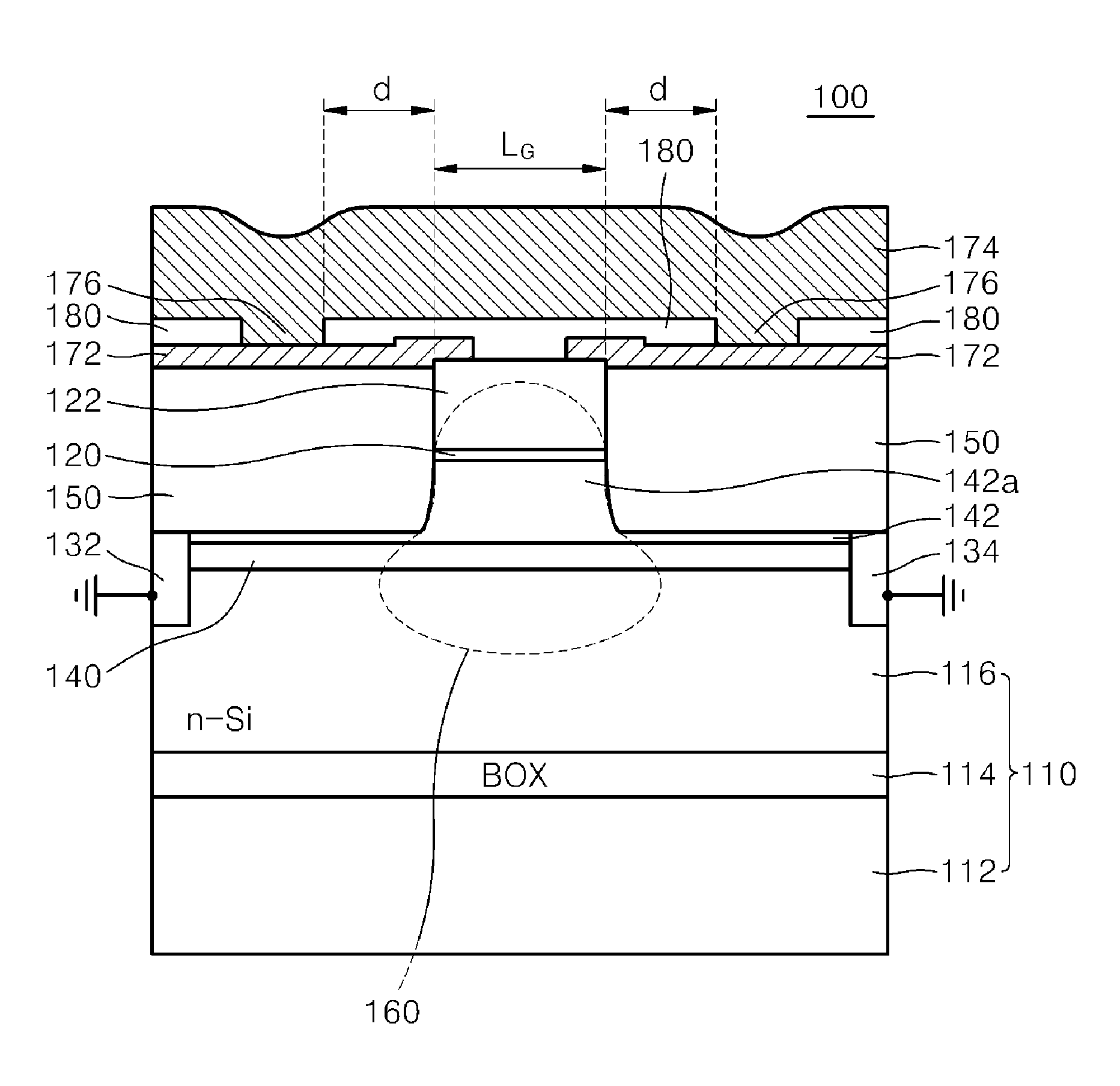
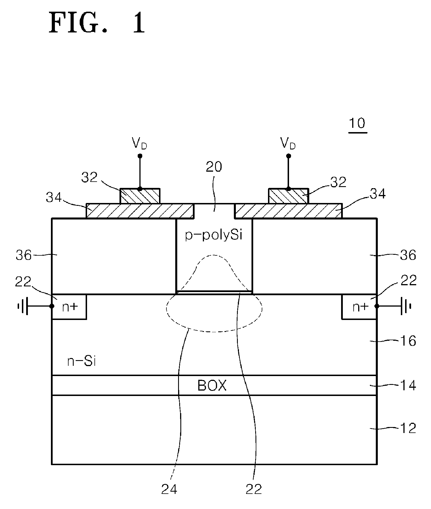
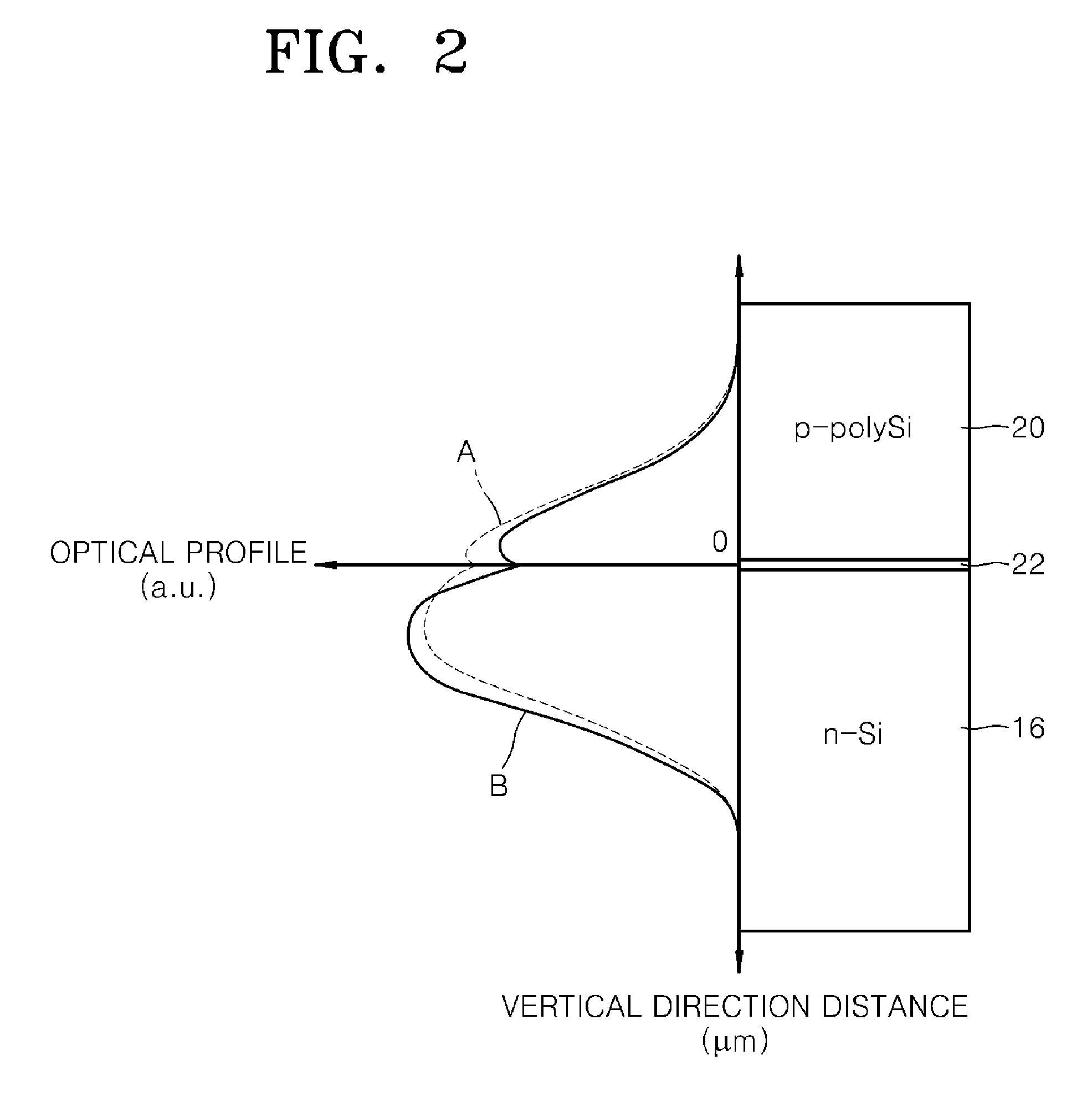
[0053]FIG. 4 shows the energy distribution around the strained buried channel area 140 of the optical device 100 of the FIG. 3 formed of the SiGe layer.

[0054]As shown in FIG. 4, if a negative voltage is applied to the gate 122, a hole channel is formed in the semiconductor cap layer 142. However, the hole channel is also formed around the strained buried channel area 140 due to an offset of a balance band. Thus, a trap density can be lowered, and a sufficient hole density can vary under a rapid switching condition.

[0055]As described above, if a phase is to be changed using holes, an optical phase modulation ratio of holes is generally approximately double that of electrons. Thus, if the second silicon layer 116 is of p-type and the high density dopant diffusion areas 132 and 134 are of p+ to change the phase using the holes, the strained buried channel area 140 may be formed of the SiGe layer to improve the mobility of the holes. Thus, the resistance of the second silicon substrate ...


PUM


Abstract

Provided is an optical device having a strained buried channel area. The optical device includes: a semiconductor substrate of a first conductive type; a gate insulating layer formed on the semiconductor substrate; a gate of a second conductive type opposite to the first conductive type, formed on the gate insulating layer; a high density dopant diffusion area formed in the semiconductor substrate under the gate and doped with a first conductive type dopant having a higher density than the semiconductor substrate; a strained buried channel area formed of a semiconductor material having a different lattice parameter from a material of which the semiconductor substrate is formed and extending between the gate insulating layer and the semiconductor substrate to contact the high density dopant diffusion area; and a semiconductor cap layer formed between the gate insulating layer and the strained buried channel area.

Description

TECHNICAL FIELD[0001]The present invention relates to a silicon photonics, and more particularly, to an optical device of a metal-insulator-semiconductor (MIS) structure.BACKGROUND ART[0002]Conventional data transmission using metal lines has limited transmission speed due to delay of a resistor-capacitor of a transmission line. In particular, the communication speed between a central processing unit (CPU) and a graphics processing unit (GPU) required for games has gradually increased. Thus, the demand for higher communication speeds has also increased. Silicon photonics has been suggested to satisfy this demand and can provide high integration. In particular, a monolithic device for optical communications can be manufactured to reliably transmit high-speed data generated inside a chip to an external chip. Also, an optical device using silicon photonics does not need to be additionally packaged, as opposed to using another device outside a chip. Thus, packaging cost can be reduced, ...

Claims


Application Information

Patent Timeline
Patent Type & Authority Patents(United States)
IPC IPC(8): H01L31/036H01L33/00
CPCG02F1/025H01L33/0037G02F1/2257H01L21/18
Inventor MHEEN, BONGKIPARK, JEONG-WOOKIM, HYUN-SOOKIM, GYUNGOCK
Owner ELECTRONICS & TELECOMM RES INST
Why Eureka
Try Eureka