Switchable high pass filter/low pass filter phase shifter having a switch circuit with FETs connected in parallel

a high-pass filter and phase shifter technology, applied in the field of switch circuits and phase shifters, can solve the problems of increasing pass loss, worsening rms phase shift error, and signal leakage from the on side to the off sid

Inactive Publication Date: 2011-04-19
RENESAS ELECTRONICS CORP
View PDF8 Cites 18 Cited by
  • Summary
  • Abstract
  • Description
  • Claims
  • Application Information

AI Technical Summary

Benefits of technology

[0035]In accordance with the present invention, DC measurement of field-effect transistors is facilitated and, when the switch circuit is turned off, a parallel resonance circuit is formed and the switch circuit can be held at a high impedance.

Problems solved by technology

At these other frequencies, the signal leaks from the ON side to the OFF side and pass loss is increased.
Furthermore, this increase in pass loss causes an undulation (up and down) in the phase angle and worsens the RMS phase-shift error, which is an indicator of the acceptability of the phase-shift quantity.

Method used


Image

  • Switchable high pass filter/low pass filter phase shifter having a switch circuit with FETs connected in parallel
  • Switchable high pass filter/low pass filter phase shifter having a switch circuit with FETs connected in parallel
  • Switchable high pass filter/low pass filter phase shifter having a switch circuit with FETs connected in parallel

Examples


first example

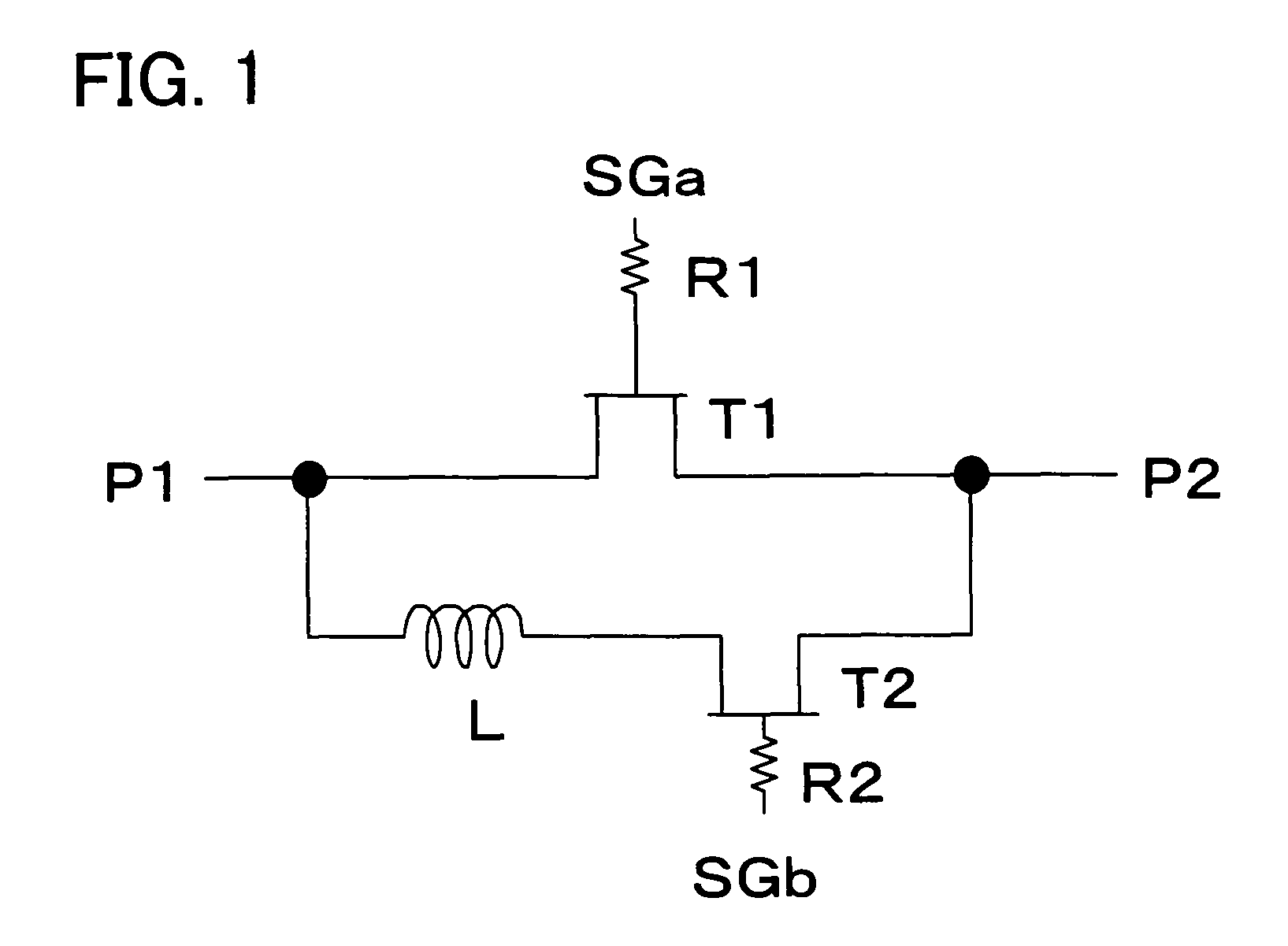
[0062]FIG. 1 is a diagram illustrating the configuration of a switch circuit according to a first example of the present invention. The switch circuit has transistors T1, T2 and an inductor L. The transistors T1, T2 are constituted by a Schottky-gate-type MESFET (Metal Semiconductor Field-Effect Transistor) or HJFET (Hetero Junction Field-Effect Transistor), etc., of GaAs or the like.

[0063]As illustrated in FIG. 1, a first end of the inductor L is connected to the drain of the transistor T1 at a node P1, the source of the transistor T2 is connected to the source of the transistor T1 at a node P2, and the second end of the inductor L is connected to the drain of the transistor T2. Further, control signals SGa, SGb are supplied to the gates of the transistors T1, T2, respectively, via respective resistor elements R1, R2 such that there will be no leakage of high-frequency signals. It goes without saying that an arrangement in which the locations of the transistor T2 and inductor L are...

second example

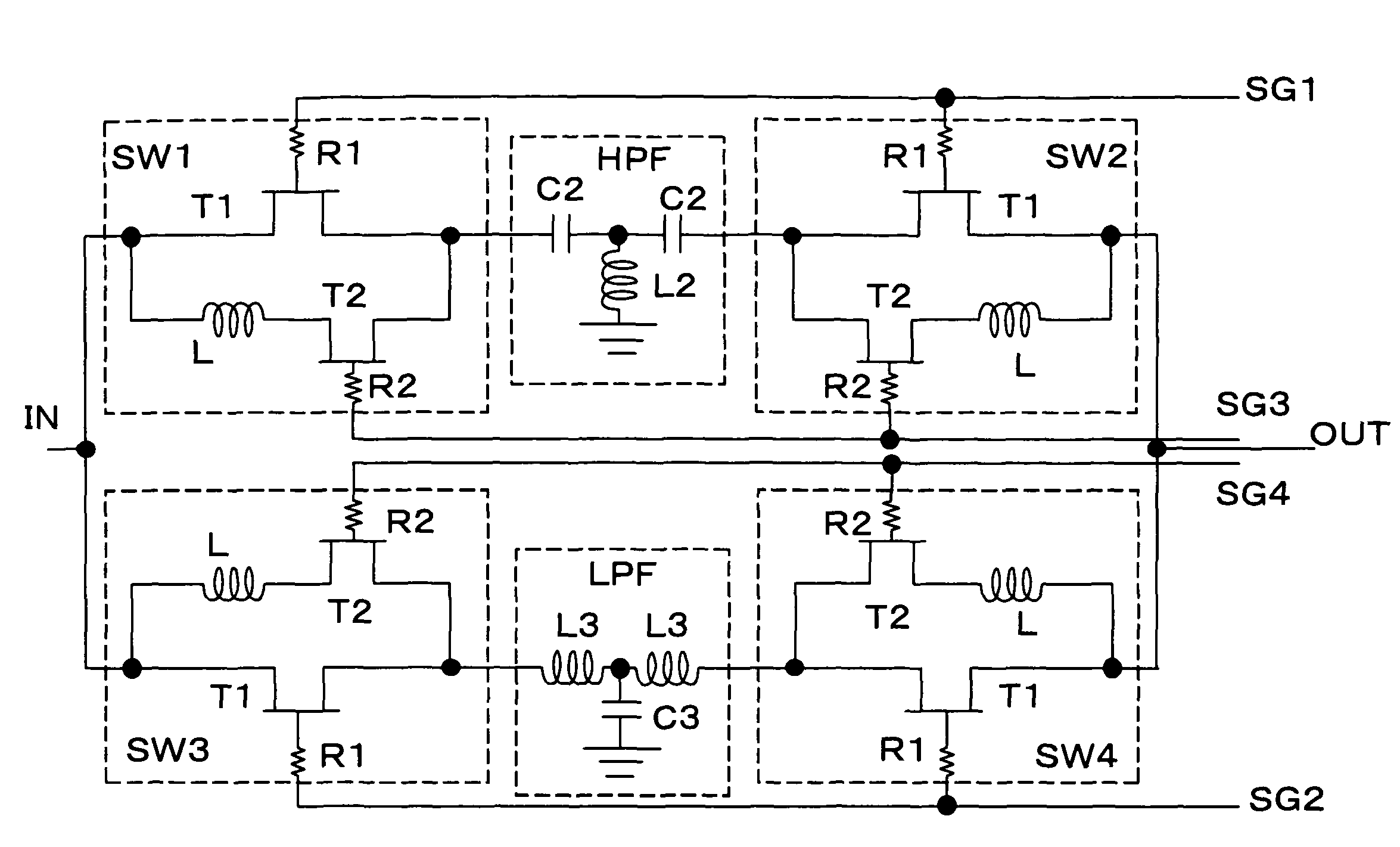
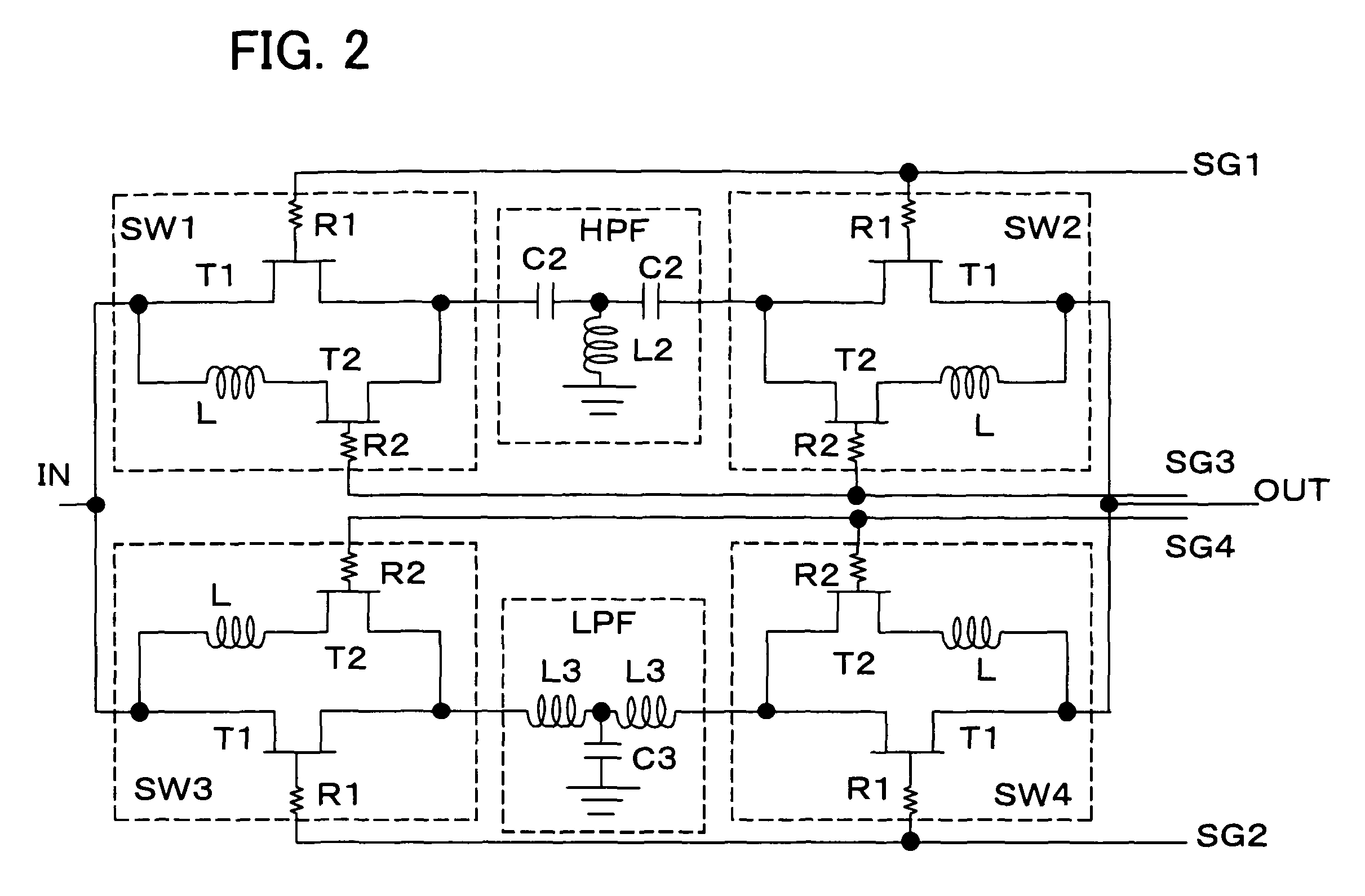
[0072]FIG. 2 is a diagram illustrating the configuration of a phase shifter according to a second example of the present invention. The phase shifter in FIG. 2 includes switch circuits SW1, SW2, SW3, SW4, a high-pass filter HPF and a low-pass filter LPF. The switch circuits SW1, SW2, SW3, SW4 are in accordance with the first example. The high-pass filter HPF has two serially connected capacitors C2 and an inductor L2 connected between the node of the two capacitors C2 and ground. The low-pass filter LPF has two serially connected inductors L3 and a capacitor C3 connected between the node of the two inductors L3 and ground.

[0073]In the phase shifter of FIG. 2, an input terminal IN is connected to an output terminal OUT via the switch circuit SW1, high-pass filter HPF and switch circuit SW2, and is connected to the output terminal OUT via the switch circuit SW3, low-pass filter LPF and switch circuit SW4.

[0074]The transistors TI in the respective switch circuits operate in contrary (e...

third example

[0080]FIG. 8 is a diagram illustrating the configuration of a phase shifter according to a third example of the present invention. Components in FIG. 8 identical with those shown in FIG. 2 are designated by like reference characters, which may not be all described in detail herein. The phase shifter of FIG. 8 is obtained by additionally providing the phase shifter of FIG. 2 with pads PAD1 to PAD6. The pad PAD1 is connected to the switch circuit SW1 and to first end of the high-pass filter HPF. The pad PAD2 is connected to the switch circuit SW2 and to second end of the high-pass filter HPF. The pad PAD3 is connected to the gates of the transistors T1 in the respective switch circuits SW1, SW2 via the resistor elements R1. The pad PAD4 is connected to the gates of the transistors T1 in the respective switch circuits SW3, SW4 via the resistor elements R1. The pad PAD5 is connected to the gates of the transistors T2 in the respective switch circuits SW1, SW2 via the resistor elements R...


PUM


Abstract

A switch circuit in which the cut-off characteristic is improved over a wide range of frequencies in the microwave band includes a first field-effect transistor functioning as a switch element, a second field-effect transistor and an inductor. A serially connected circuit composed of the inductor and second field-effect transistor is connected in parallel with the first field-effect transistor across the source and drain thereof. The second field-effect transistor is turned on when the first field-effect transistor operates normally and is turned off when the first field-effect transistor is inspected.

Description

REFERENCE TO RELATED APPLICATION[0001]This application is based upon and claims the benefit of the priority of Japanese patent application No. 2007-215542 filed on Aug. 22, 2007, the disclosure of which is incorporated herein in its entirety by reference thereto.TECHNICAL FIELD[0002]This invention relates to a switch circuit and phase shifter. More particularly, the invention relates to a microwave-band switch circuit and to a phase shifter that uses this switch circuit.BACKGROUND[0003]Several types of phase shifters exist. For example, a line-switching-type phase shifter is known in which 50Ω-lines of different lengths are connected by two SPDTs (single-pole, double-throw) switches and the difference in the electrical lengths of the two lines obtained by switching is used as the amount of phase shift. There is also a filter-switching-type phase shifter in which a plurality of inductances or capacitances of a lumped constant and SPDT switches are combined and use is made of a phase ...

Claims


Application Information

Patent Timeline
Patent Type & Authority Patents(United States)
IPC IPC(8): H01P1/18H01P1/15
CPCH03H11/16H01P1/18
Inventor ATSUMO, TAKAO
Owner RENESAS ELECTRONICS CORP
Why Eureka
Try Eureka