Curvature-compensated band-gap voltage reference circuit

a voltage reference circuit and curvature compensation technology, applied in the direction of power conversion systems, instruments, dc-dc conversion, etc., can solve the problems of special steps to be taken and the component cost is too high for many applications

Active Publication Date: 2011-04-26
APTIV TECH LTD
View PDF5 Cites 14 Cited by
  • Summary
  • Abstract
  • Description
  • Claims
  • Application Information

AI Technical Summary

Problems solved by technology

Also, special steps must be taken to minimize stresses caused by the circuit packaging because package stress non-uniformity can introduce additional voltage instability over time.
Conventional approaches for addressing the curvature compensation and package stress issues typically result in a component cost that is too high for many applications.

Method used


Image

  • Curvature-compensated band-gap voltage reference circuit
  • Curvature-compensated band-gap voltage reference circuit
  • Curvature-compensated band-gap voltage reference circuit

Examples


Embodiment Construction

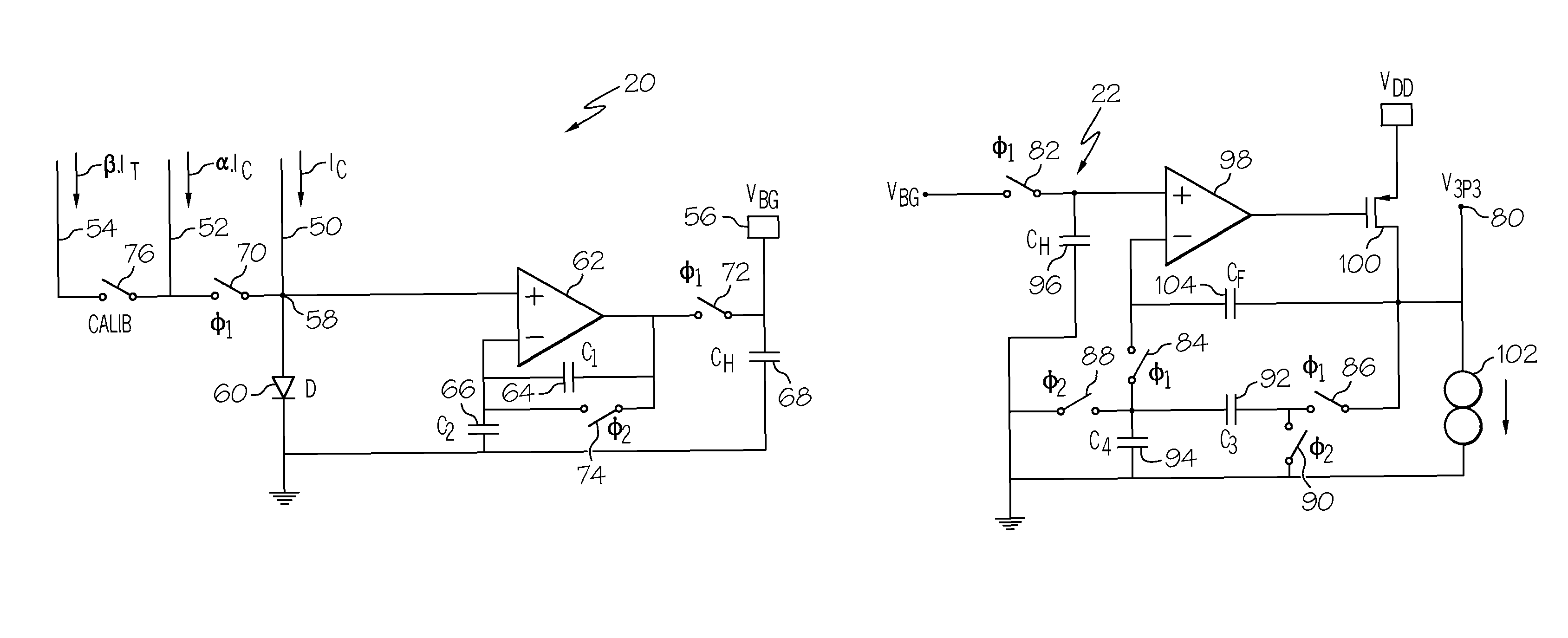
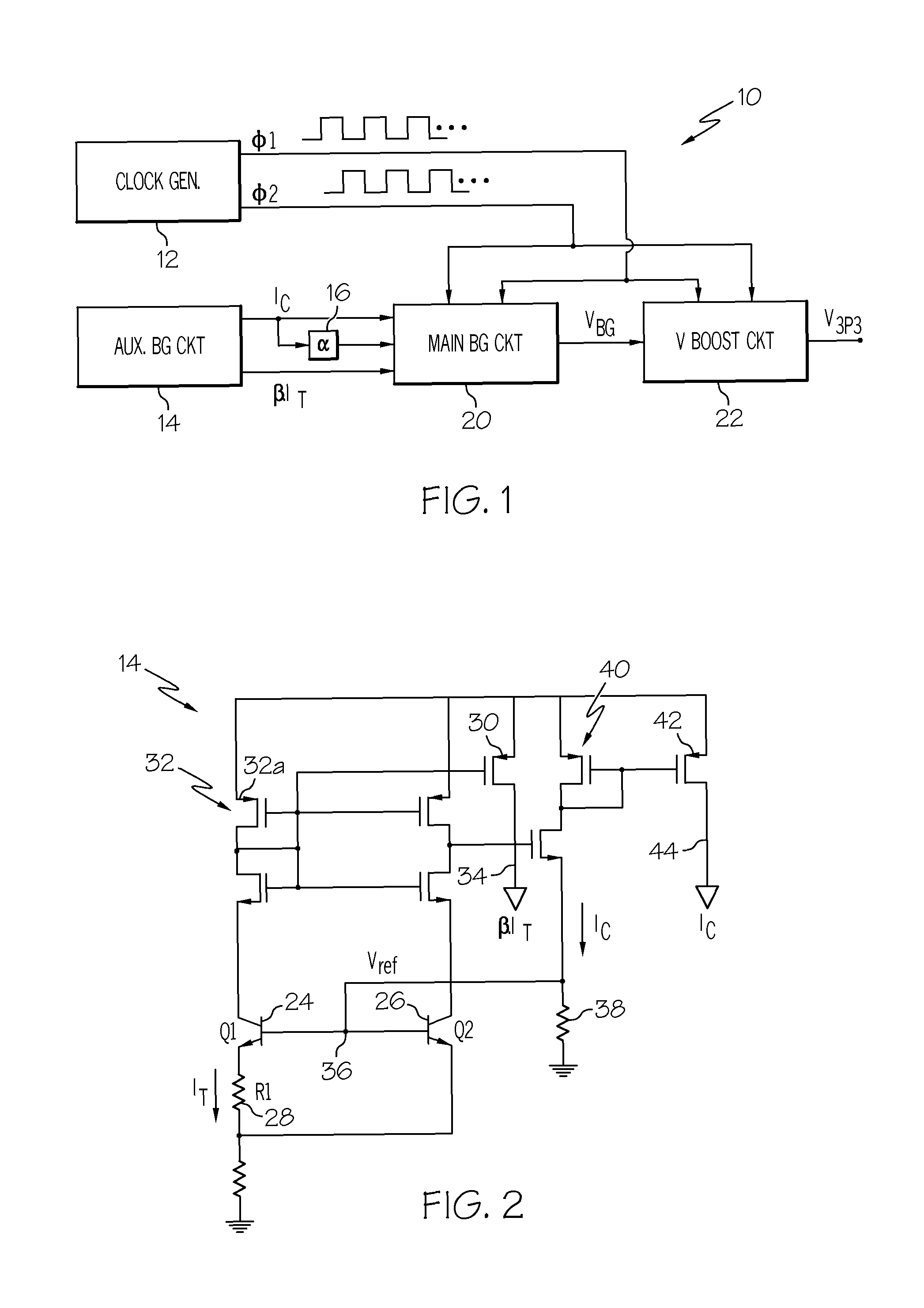
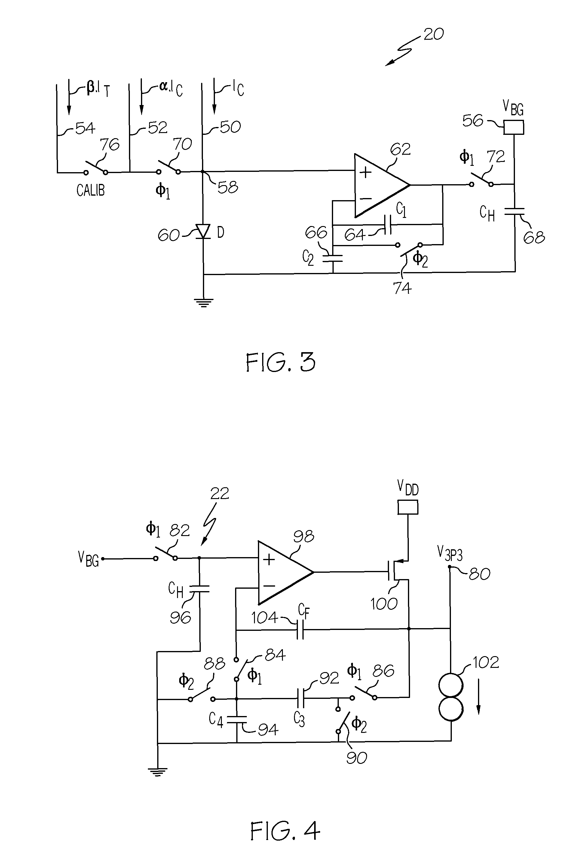
[0010]Referring to the drawings, and particularly to FIG. 1, the reference numeral 10 generally designates a high-precision curvature-compensated band-gap voltage reference circuit according to this invention, including a two-phase clock generator 12, an auxiliary band-gap circuit 14, a trimable scaling parameter 16, a main band-gap circuit 20, and a voltage-boost circuit 22. The clock generator develops a pair of fixed-frequency non-overlapping opposite-phase square-wave signals φ1 and φ2 for the main band-gap and voltage-boost circuits 20 and 22. The auxiliary band-gap circuit 14, described in detail below in reference to FIG. 2, develops two signals needed by the main band-gap circuit 20, which signals may be developed by some other means if desired. The signals developed by auxiliary band-gap circuit 14 are current signals, and include: a substantially constant current IC, and a scaled current β·IT that is proportional-to-absolute-temperature (PTAT). The block 16 generates a tri...


PUM


Abstract

A band-gap reference voltage is developed by a phase-clocked band-gap circuit including a single PN junction through which first and second constant currents are alternately directed. A current proportional to absolute temperature is selectively added to one of the first and second constant currents to curvature-compensate the developed band-gap reference voltage. The band-gap circuit is calibrated at any desired temperature by interrupting the curvature compensation current and trimming the one constant current to bring the un-compensated band-gap reference voltage into correspondence with a nominal band-gap voltage functionally related to the calibration temperature and circuit component values.

Description

TECHNICAL FIELD[0001]The present invention relates to voltage reference circuits, and more particularly to a low-cost high-precision curvature-compensated band-gap voltage reference circuit.BACKGROUND OF THE INVENTION[0002]Band-gap voltage reference circuits are routinely used in integrated circuit applications that require a reference voltage that is reasonably precise and stable over a range of temperatures. Fundamentally, a band-gap voltage reference circuit includes two bipolar base-emitter junctions operating at different current densities. The reference voltage is obtained by summing one of the base-emitter voltages with a scaled difference of the two base-emitter voltages. Since the base-emitter voltage is inversely proportional to temperature and the scaled difference voltage is directly proportional to temperature, their sum is temperature independent to the first order. However, the reference voltage still exhibits some second and higher order nonlinearity (curvature) with...

Claims


Application Information

Patent Timeline
Patent Type & Authority Patents(United States)
IPC IPC(8): G05F1/10
CPCH02M3/073
Inventor ZARABADI, SEYED R.
Owner APTIV TECH LTD
Why Eureka
Try Eureka