Manufacturing method of a photoelectric conversion device

a technology of photoelectric conversion and manufacturing method, which is applied in the direction of semiconductor devices, diodes, electrical devices, etc., can solve the problems of photodiodes sustain etching damage, and achieve the effect of improving the control precision of the offset of a protection area and reducing the amount of etching damag

Inactive Publication Date: 2011-05-03
CANON KK
View PDF17 Cites 29 Cited by
  • Summary
  • Abstract
  • Description
  • Claims
  • Application Information

AI Technical Summary

Benefits of technology

[0014]The present invention provides a method for reducing the amount of etching damage sustained by the photoelectric conversion unit, and for improving the control precision of the offset of a protection area of the photoelectric conversion unit from the gate electrode of a transfer transistor in a photoelectric conversion device.
[0016]According to the present invention, it is possible to reduce the etching damage sustained by a photoelectric conversion unit and to improve the control precision of the offset of a protection region of the photoelectric conversion unit from a gate electrode of a transfer transistor in a photoelectric conversion device.

Problems solved by technology

However, in the technique of Japanese Patent Laid-Open No. 2005-123517, there is a possibility that the photodiode sustains etching damage when removing the film that masks the photodiode or the photoresist by etching after the process to form the side spacer 1111 is finished.

Method used


Image

  • Manufacturing method of a photoelectric conversion device
  • Manufacturing method of a photoelectric conversion device
  • Manufacturing method of a photoelectric conversion device

Examples


Embodiment Construction

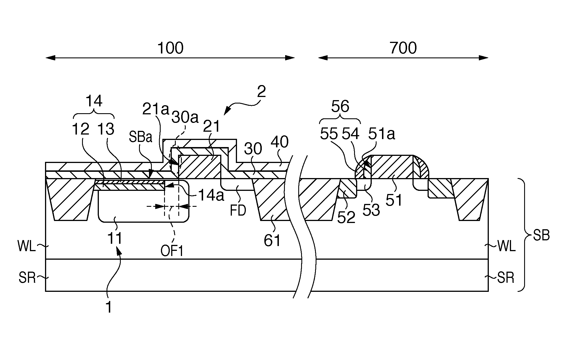
[0024]The overall structure of the photoelectric conversion device 800 according to an embodiment of the present invention will be explained using FIG. 1. FIG. 1 is a diagram illustrating the structure of the photoelectric conversion device 800 according to an embodiment of the present invention.

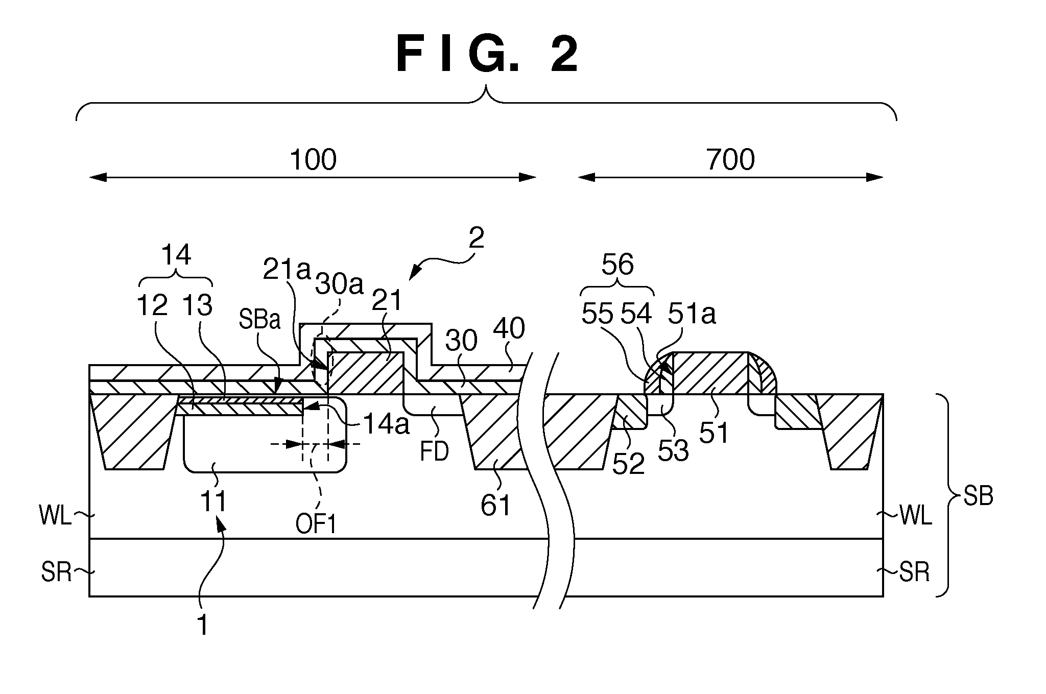
[0025]The photoelectric conversion device 800 has a pixel array region 100 and peripheral region 700. The pixel array region 100 is a region in which a plurality of pixels are arrayed. The peripheral region 700 is a region arranged in the peripheral region of the pixel array region 100, and is a region in which a plurality of control circuits are arranged. Each of the plurality of control circuits includes a MOS transistor for controlling a plurality of pixels and a circuit that acts as a readout path.

[0026]A plurality of pixels 6 are arranged in a direction along rows and in a direction along columns in the pixel array region 100.

[0027]Each pixel 6 includes a photoelectric conversion unit 1...


PUM


Abstract

A manufacturing method of a photoelectric conversion device included a first step of forming a gate electrode, a second step of forming a semiconductor region of a first conductivity type, a third step of forming an insulation film, and a fourth step of forming a protection region of a second conductivity type, which is the opposite conductivity type to the first conductivity type, by implanting ions in the semiconductor region using the gate electrode of the transfer transistor and a portion covering a side face of the gate electrode of the transfer transistor of the insulation film as a mask in a state in which the semiconductor substrate and the gate electrode of the transfer transistor are covered by the insulation film, and causing a portion of the semiconductor region of the first conductivity type from which the protection region is removed to be the charge accumulation region.

Description

BACKGROUND OF THE INVENTION[0001]1. Field of the Invention[0002]The present invention relates to the manufacturing method of a photoelectric conversion device.[0003]2. Description of the Related Art[0004]As shown in FIG. 1 of Japanese Patent Laid-Open No. 2005-123517, installing an n-layer 104 that is an n-type semiconductor region for accumulating charges and a p-layer 105 that is a p-type semiconductor region on that n-layer 104 in a photodiode of a solid-state imaging device is described in Japanese Patent Laid-Open No. 2005-123517. According to Japanese Patent Laid-Open No. 2005-123517, it is possible to suppress the dark current on the light-receiving surface of the photodiode by this structure.[0005]Installing a bypass region 106 that continuously extends from the n-layer 104 to the bottom of the gate region 103 (control electrode) of a transfer MOS transistor is disclosed in Japanese Patent Laid-Open No. 2005-123517. The width of this bypass region 106 is controlled by implan...

Claims


Application Information

Patent Timeline
Patent Type & Authority Patents(United States)
IPC IPC(8): H01L21/266H01L21/339
CPCH01L27/14603H01L27/307H01L27/14689H01L27/14625H01L27/14643H10K39/32
Inventor MISHIMA, RYUICHISHIMOTSUSA, MINEONARUSE, HIROAKI
Owner CANON KK
Why Eureka
Try Eureka