Chip resistor and its manufacturing method

a technology of resistor and manufacturing method, which is applied in the direction of resistor details, resistor chip manufacturing, resistor 201, etc., can solve the problems of unfavorable enhancement of surge resistance of chip resistor, time-consuming and labor-intensive, and likely failure of chip resistor, so as to reduce the time required for forming grooves by trimming, reduce the effect of thermal expansion or contraction of insulating substrate, and reduce the time required for soldering

Active Publication Date: 2011-05-10
ROHM CO LTD
View PDF15 Cites 10 Cited by
  • Summary
  • Abstract
  • Description
  • Claims
  • Application Information

AI Technical Summary

Benefits of technology

[0024]According to the present invention, defective soldering due to the thermal expansion or contraction of the insulating substrate is reduced, and the current flow path can be long and narrow, to provide enhanced surge resistance. Further, the time required for forming a groove by trimming is reduced, which contributes to reduction in manufacturing cost.

Problems solved by technology

With a short current flow path, breakage or deterioration of the chip resistor is likely to occur due to the application of instantaneous high voltage or surge voltage, and in this sense the arrangement of the chip resistor 201 is unfavorable for enhancement of the surge resistance.
Another problem is as follows.
To forma longer trimming groove, however, takes a longer process time and gives rise to a cost increase.

Method used


Image

  • Chip resistor and its manufacturing method
  • Chip resistor and its manufacturing method
  • Chip resistor and its manufacturing method

Examples


first embodiment

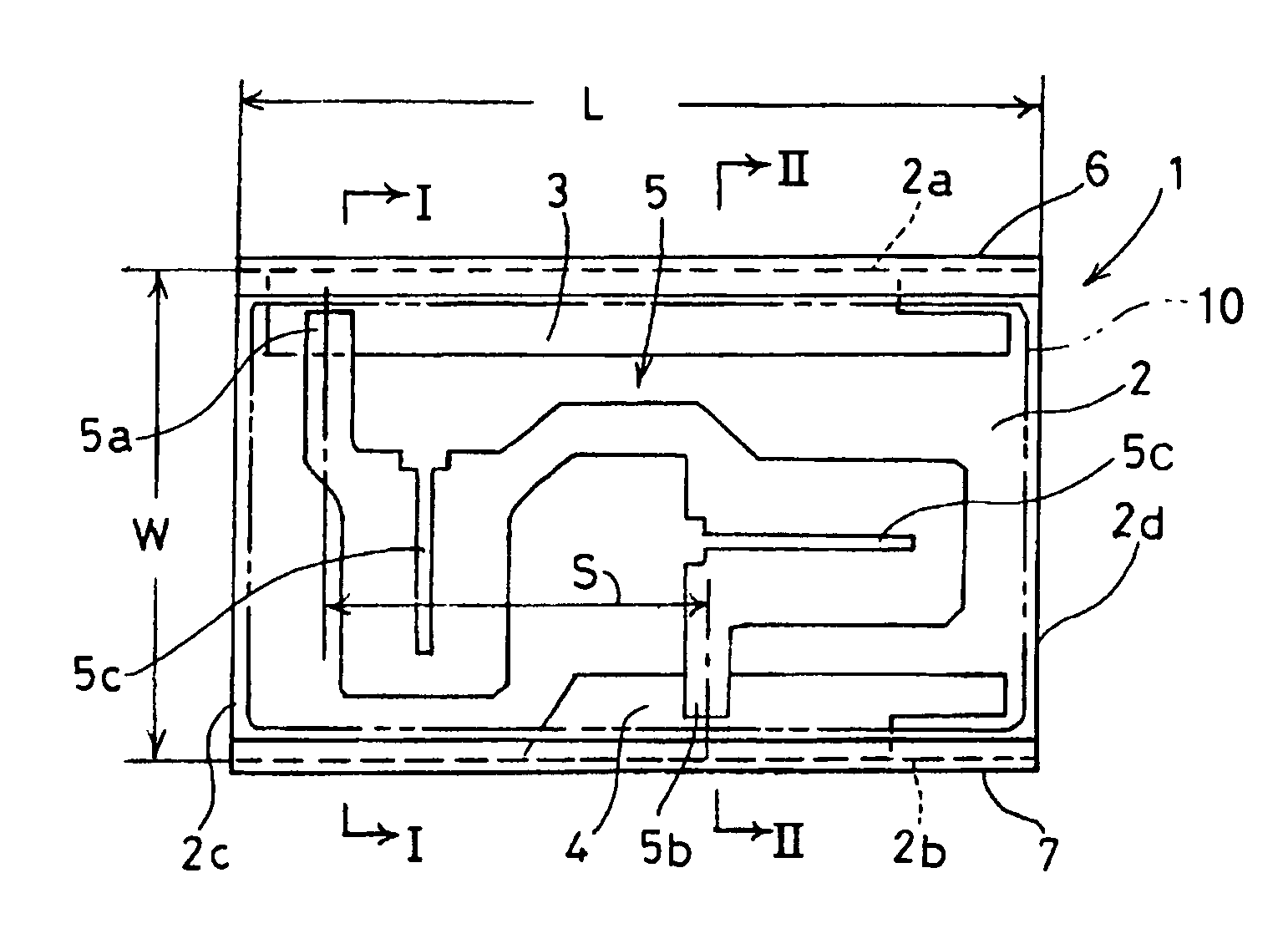
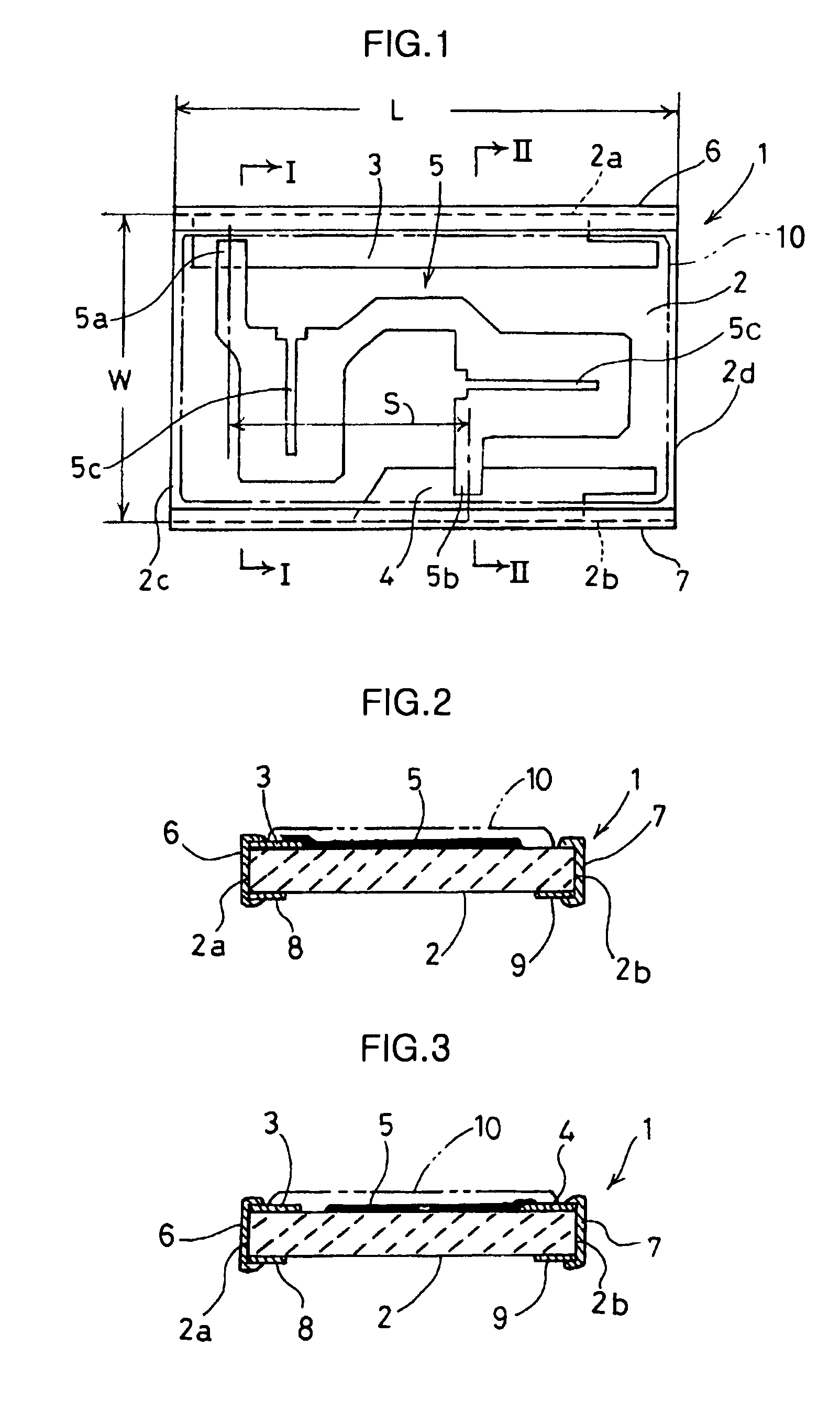
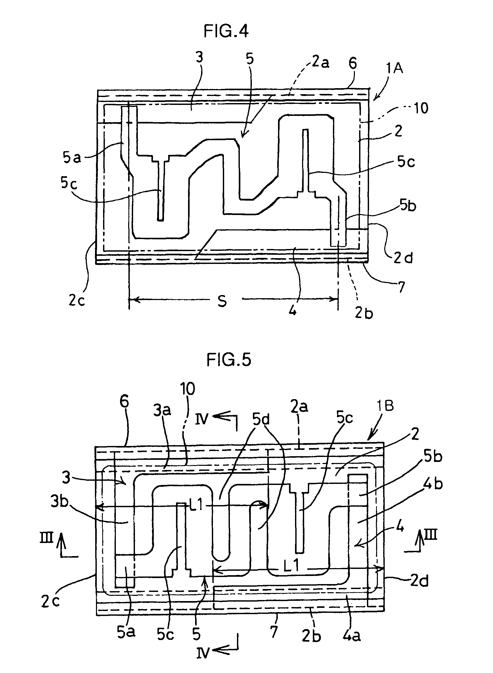
[0042]FIGS. 1-3 show a chip resistor according to the present invention.

[0043]The chip resistor 1 according to the first embodiment at least includes an insulating substrate 2, a pair of upper electrodes 3 and 4, a resistor film 5, a pair of terminal electrodes 6 and 7, a pair of lower electrodes 8 and 9 and a cover coat 10.

[0044]The insulating substrate 2 is made of a heat-resistant insulating material such as a ceramic material and in the form of a chip having an elongated rectangular shape with a longer side L and a shorter side W. The upper electrode 3 is in the form of a strip formed on the upper surface of the insulating substrate 2 at a portion adjacent to a longer side surface 2a to extend along the longer side surface 2a. The upper electrode 4 is in the form of a strip formed on the upper surface of the insulating substrate 2 at a portion adjacent to a longer side surface 2b to extend along the longer side surface 2b. The resistor film 5 is formed between the upper electrod...


PUM

PropertyMeasurementUnit
distanceaaaaaaaaaa
lengthaaaaaaaaaa
meandering shapeaaaaaaaaaa

Abstract

A chip resistor (1) according to the present invention includes an insulating substrate (2) which is in the form of an elongated rectangle in plan view, a pair of upper electrodes (3, 4) in the form of a strip formed on the upper surface of the insulating substrate (2) at portions adjacent to the long side surfaces of the insulating substrate to extend along the side surfaces, a resistor film (5) formed on the upper surface of the insulating substrate (2) and electrically connected to the upper electrodes (3, 4), and a pair of terminal electrodes (6, 7) formed on the two long side surfaces of the insulating substrate and electrically connected to the upper electrodes (3, 4), respectively. One of two longitudinal ends of the resistor film (5) is connected to one of the upper electrodes (3), whereas the other one of the two longitudinal ends of the resistor film is connected to the other one of the upper electrodes (4). The connection position at which the resistor film (5) is connected to the one of the upper electrodes (3) and the connection position at which the resistor film (5) is connected to the other one of the upper electrodes (4) are spaced from each other by a predetermined distance in the longitudinal direction of the upper surface of the insulating substrate (2).

Description

TECHNICAL FIELD[0001]The present invention relates to a chip resistor having high surge resistance, and also to a method for manufacturing such a chip resistor.BACKGROUND ART[0002]Chip resistors in general include an insulating substrate and terminal electrodes for soldering, where the substrate appears to be an elongated rectangle as viewed in plan, and each of the terminal electrodes is formed on one of the two end surfaces adjacent to the shorter sides of the elongated rectangle.[0003]FIG. 15 is a perspective view showing a typical chip resistor. The chip resistor 101 includes an insulating substrate 102 whose upper surface is formed with upper electrodes 103 and 104 disposed at the ends of the upper surface spaced from each other in the longitudinal direction of the substrate. The upper surface of the substrate 102 is also formed with a resistor film 105 extending in the longitudinal direction of the insulating substrate 102. The ends of the resistor film 105 overlap the upper e...

Claims


Application Information

Patent Timeline
Patent Type & Authority Patents(United States)
IPC IPC(8): H01C1/012
CPCH01C1/012H01C17/006H01C1/142Y10T29/49099
Inventor YONEDA, MASAKI
Owner ROHM CO LTD
Why Eureka
Try Eureka