Pre-aligned metrology system and modules

a metrology system and module technology, applied in the field of optical metrology, can solve the problems of further complications, challenge for sem to meet the metrology request, etc., and achieve the effect of improving the reliability and availability of the ims

Inactive Publication Date: 2011-05-10
TOKYO ELECTRON LTD
View PDF16 Cites 0 Cited by
  • Summary
  • Abstract
  • Description
  • Claims
  • Application Information

AI Technical Summary

Benefits of technology

[0010]The invention presents a Pre-Aligned Metrology Assembly that can be used in an integrated metrology sensor (IMS) that is configured using a plurality of Field Replaceable Units (FRUs). The invention presents a Pre-Aligned Metrology Assembly that is compact and well suited for integration into a compact IMS. The IMS can include one or more Pre-Aligned Metrology Assemblies, and the IMS can be used to measure structures 50 nm wide or smaller. The Pre-Aligned Metrology Assembly can be pre-aligned and calibrated so that it can be swapped in the field with minimum amount of time. The Pre-Aligned Metrology Assembly can be swapped as part of scheduled maintenance to improve the reliability and availability of the IMS.

Problems solved by technology

Traditionally the inspection of CDs that are smaller than the wavelength of visible light has been done using large and expensive scanning electron microscopes (SEM).
It is a very challenging for SEM to meet the metrology request in these cases.
The wafer may also be loaded into the measurement tool at an arbitrary angle creating further complications for instruments that have a preferred measurement orientation with respect to certain wafer features.
As the semiconductor roadmap goes to smaller and smaller nodes, more and more challenges on semiconductor process control to meet very tight tolerance while the structure becomes smaller.

Method used


Image

  • Pre-aligned metrology system and modules
  • Pre-aligned metrology system and modules
  • Pre-aligned metrology system and modules

Examples


Embodiment Construction

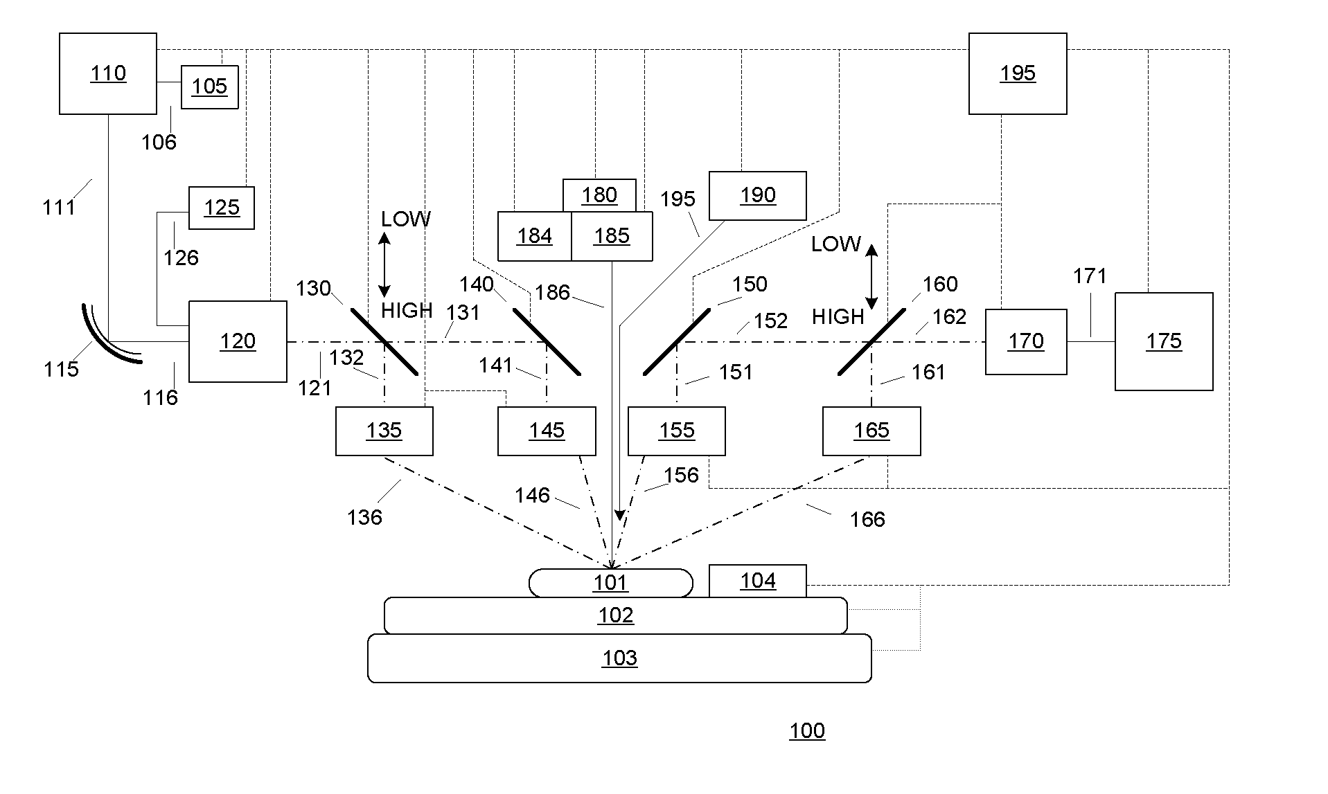
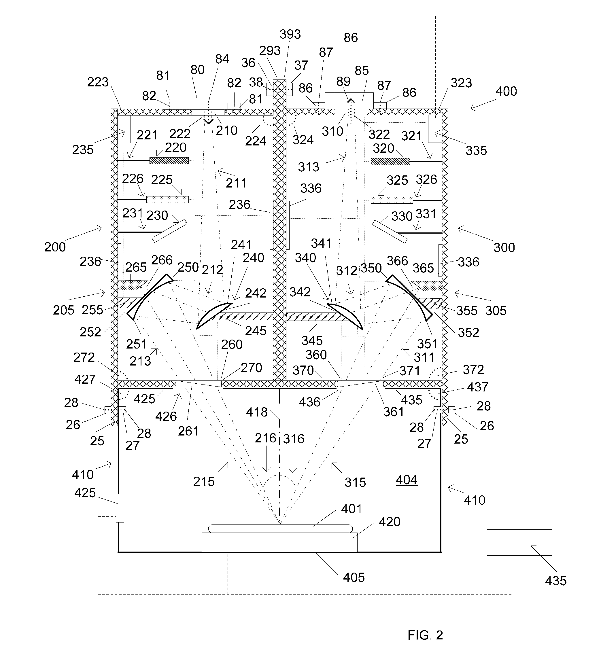
[0015]Reliability, availability, and performance are the most important parameters for semiconductor equipments in a modern fabrication environment. Many semiconductor manufacturers use optical metrology systems for thin-film and optical CD measurements that include stand-alone tools, and use off-line applications for process monitoring. As the semiconductor roadmap goes to smaller and smaller nodes, the tightened tolerances associated with the smaller structures become more challenging to obtain and verify using semiconductor process control applications. Thus, integrated metrology tools are required to meeting measurement time and accuracy on the smaller structures made on the wafer. In addition, the measured data from the integrated metrology sensor (IMS) can be used either to optimize the process tools that are being used to create the structures on the wafer, or to adjust the process tool conditions that are being used to further process the wafer. When the metrology tool is in...


PUM


Abstract

A Pre-Aligned Metrology System comprising a number of Pre-Aligned Metrology Assemblies and Pre-Aligned Metrology Modules for measuring a target on a wafer. The Pre-Aligned Metrology Assemblies and Pre-Aligned Metrology Modules can reduce the maintenance down time and decrease the cost of ownership (COO).

Description

BACKGROUND OF THE INVENTION[0001]1. Field of the Invention[0002]The present invention relates to optical metrology, and more particularly to improving the optical metrology process using a pre-aligned metrology system that includes pre-aligned metrology assemblies and pre-aligned metrology modules.[0003]2. Description of the Related Art[0004]In the manufacture of integrated circuits, very thin lines or holes down to 10 nm or sometimes smaller are patterned into photoresist and then transferred using an etching process into a layer of material below on a silicon wafer. It is extremely important to inspect and control the width and profile (also known as critical dimensions or CDs) of these lines or holes. Traditionally the inspection of CDs that are smaller than the wavelength of visible light has been done using large and expensive scanning electron microscopes (SEM). As the structures patterned get smaller and smaller, the measurement precision and accuracy becomes much higher, and...

Claims


Application Information

Patent Timeline
Patent Type & Authority Patents(United States)
IPC IPC(8): G01B11/00
CPCG03F7/70625G01B11/27
Inventor LI, SHIFANG
Owner TOKYO ELECTRON LTD
Why Eureka
Try Eureka