Light emitting device

a technology of light-emitting devices and light-emitting devices, which is applied in the direction of semiconductor devices, basic electric elements, electrical appliances, etc., can solve the problems of unsatisfactory efficiency of light extraction above the light-emitting devices, and achieve the effect of reducing the amount of light, reducing the yield, and improving the optical extraction efficiency of the whole devi

Inactive Publication Date: 2011-06-07
MATSUSHITA ELECTRIC WORKS LTD
View PDF35 Cites 96 Cited by
  • Summary
  • Abstract
  • Description
  • Claims
  • Application Information

AI Technical Summary

Benefits of technology

[0003]In view of the above problem, the present invention has been accomplished and has an object of providing a light emitting device which is capable of improving its optical output.

Problems solved by technology

However, the above light emitting device is found unsatisfactory in extracting the light efficiently because of that the light radiated from the side faces of the LED chip is absorbed in the circuit board, or leaked through a junction between the frame and the circuit board.

Method used


Image

  • Light emitting device
  • Light emitting device
  • Light emitting device

Examples


Embodiment Construction

[0023]Hereinafter, the present invention will be explained in detail with reference to the attached drawings.

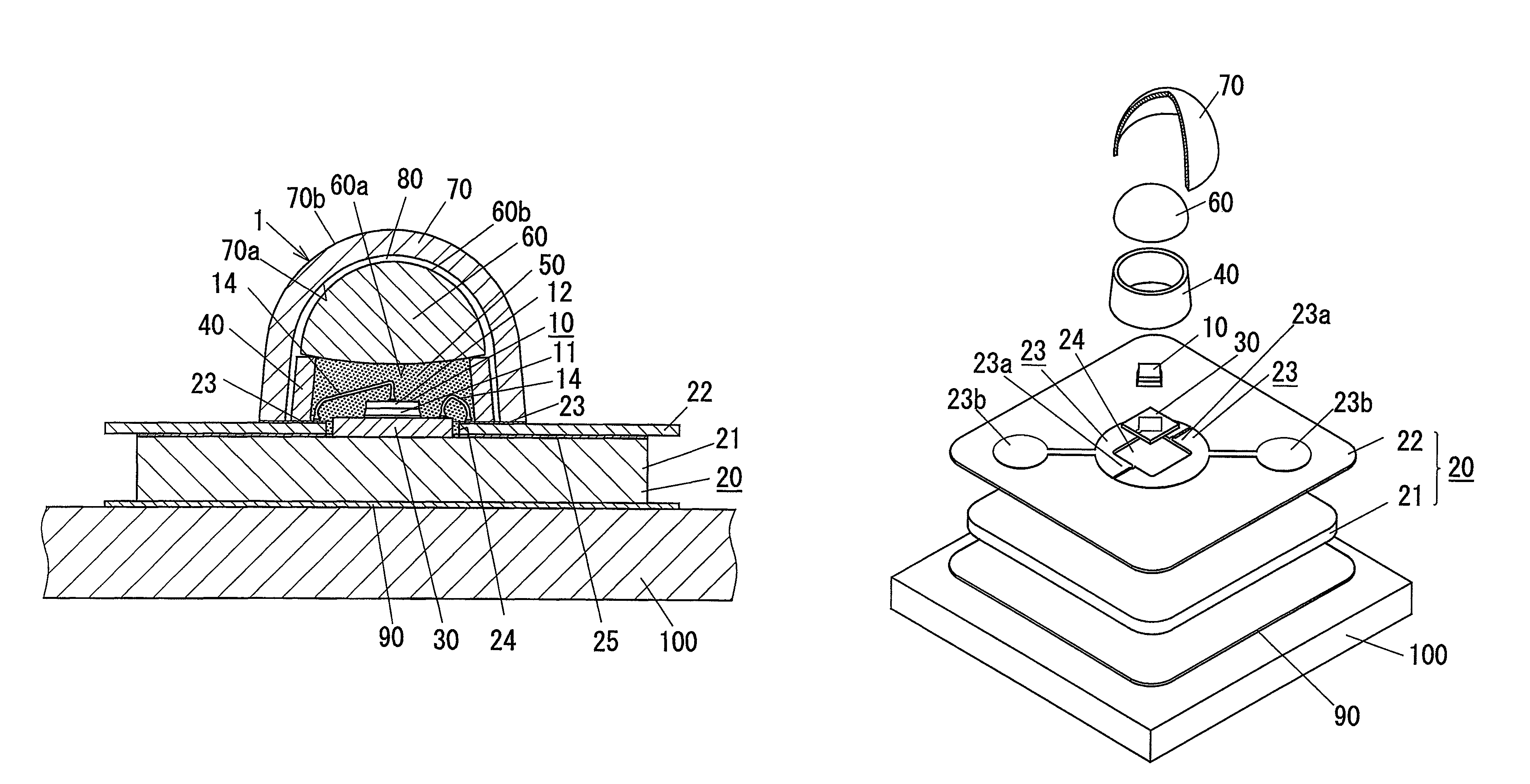
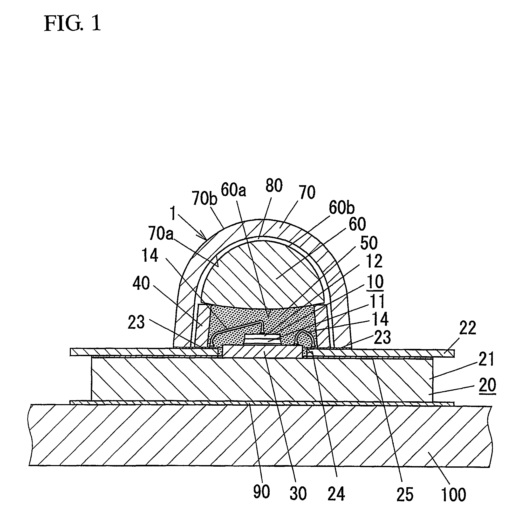
[0024]As shown in FIGS. 1 and 2, a light emitting device 1 in accordance the present embodiment comprises an LED chip 10, a circuit board 20 made of a thermally conductive material to mount the LED chip 10 thereon, a frame 40 surrounding the LED chip 10 on the surface of the circuit board 20, an encapsulation member 50 which is elastic and is made of a translucent material (transparent resin) filled within the frame 40 to encapsulate the LED chip 10 and bonding wires 14 connected to the LED chip 10, a lens 60 superimposed on the encapsulation member 50, and a dome-shaped color conversion member 70 which is a molded member molded from a transparent material mixed with a fluorescent material and disposed on the circuit board 20 to cover the lens 60. The light emitting device 1 of the present embodiment is adapted in use, for example, as a light source for an illumination applia...


PUM


Abstract

A light emitting device includes a light emitting diode chip, a heat conductive plate mounting thereon the light emitting diode chip, a sub-mount member disposed between said light emitting diode chip and said heat conductive plate, a dielectric substrate stacked on the heat conductive plate and being formed with a through-hole through which the sub-mount member is exposed, an encapsulation member for encapsulation of said light emitting diode chip, and a lens superimposed on the encapsulation member. The sub-mount member is formed around a coupling portion of the light emitting diode chip with a reflective film which reflects a light emitted from a side face of the light emitting diode chip. The sub-mount member is selected to have a thickness such that the reflecting film has its surface spaced away from said heat conductive plate by a greater distance than said dielectric substrate.

Description

TECHNICAL FIELD[0001]The invention relates to a light emitting device using a LED (Light Emitting Diode) chip.BACKGROUND ART[0002]Japanese Unexamined Patent Application Publication No. 2001-85748 (hereinafter referred to as patent document 1) and Japanese Unexamined Patent Application Publication No. 2001-148514 (hereinafter referred to as patent document 2) propose a light emitting device which comprises a LED chip, a circuit board mounting the LED chip, a metal frame (e.g. made of aluminum) surrounding the LED chip on the surface of the circuit board, an encapsulation member (e.g. made of transparent resin such as epoxy resin and silicone resin) filled within the frame to encapsulate the LED chip and bonding wires connected to the LED chip. The frame disclosed in the Patent document 1 and 2 is shaped to have an opening area which becomes greater as it is spaced away from the circuit board and is finished to have a mirror interior face which serves as a reflector reflecting a light...

Claims


Application Information

Patent Timeline
Patent Type & Authority Patents(United States)
IPC IPC(8): H01L33/48H01L33/50H01L33/58H01L33/60H01L33/64
CPCH01L33/483H01L33/505H01L33/642H01L33/58H01L33/60H01L33/507H01L2224/48091H01L2224/73265H01L2924/19107H01L2224/45144H01L2924/00014H01L2924/00
Inventor KAMADA, KAZUONISHIOKA, YASUSHIURANO, YOUJI
Owner MATSUSHITA ELECTRIC WORKS LTD
Why Eureka
Try Eureka