

Semiconductor device and manufacturing method thereof
a technology of semiconductor devices and manufacturing methods, applied in semiconductor devices, semiconductor/solid-state device details, electrical apparatus, etc., can solve the problems of complex stress including shear stress inside the device, speed up the processing rate, and difficult to realize the dielectric constant reduction required for the next generation and future generations, etc., to achieve small design constraints and high reliability. , the effect of high manufacturing yield
- Summary
- Abstract
- Description
- Claims
- Application Information
AI Technical Summary
Benefits of technology
Problems solved by technology
Method used
Image

Examples
example 1
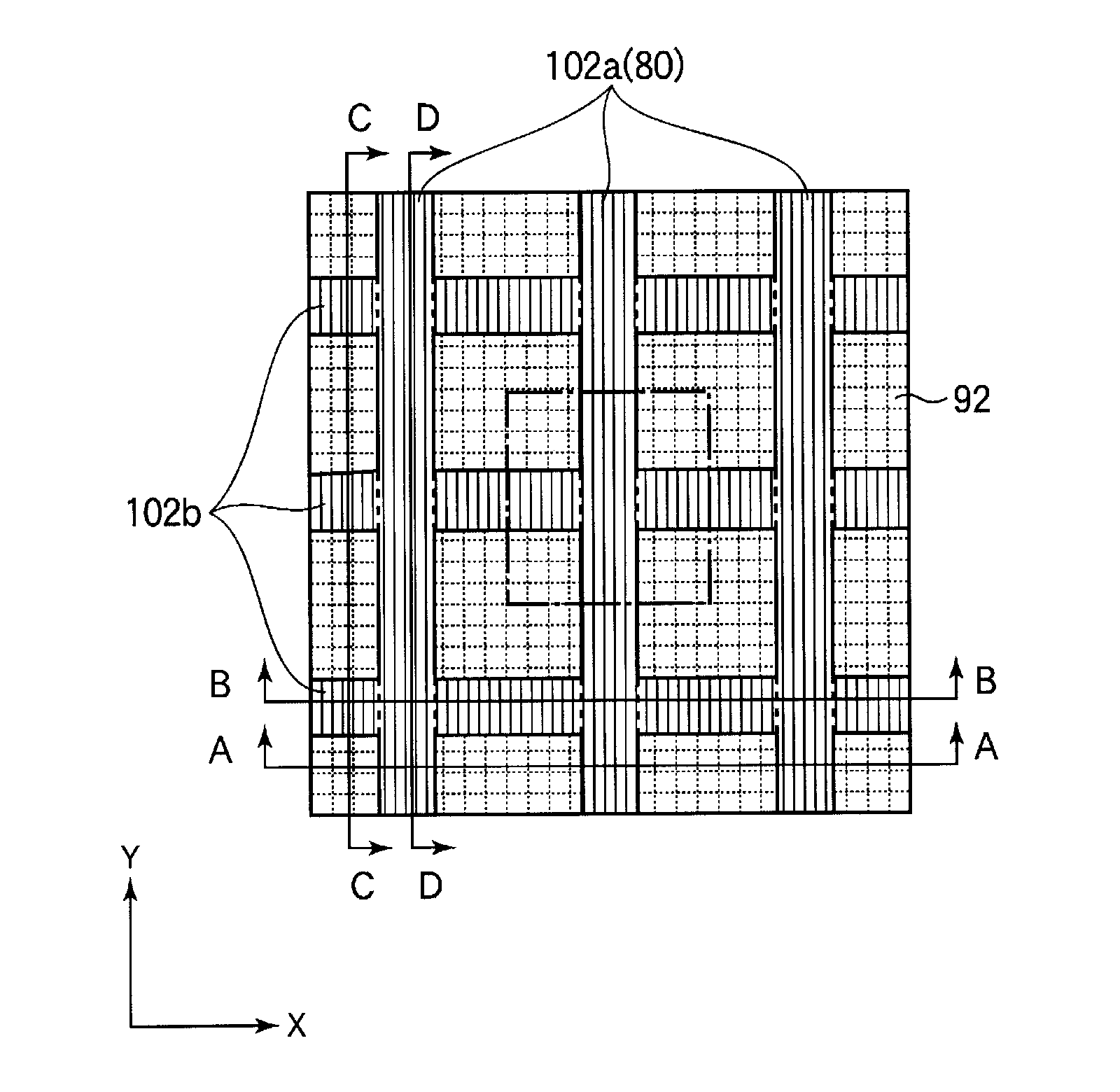
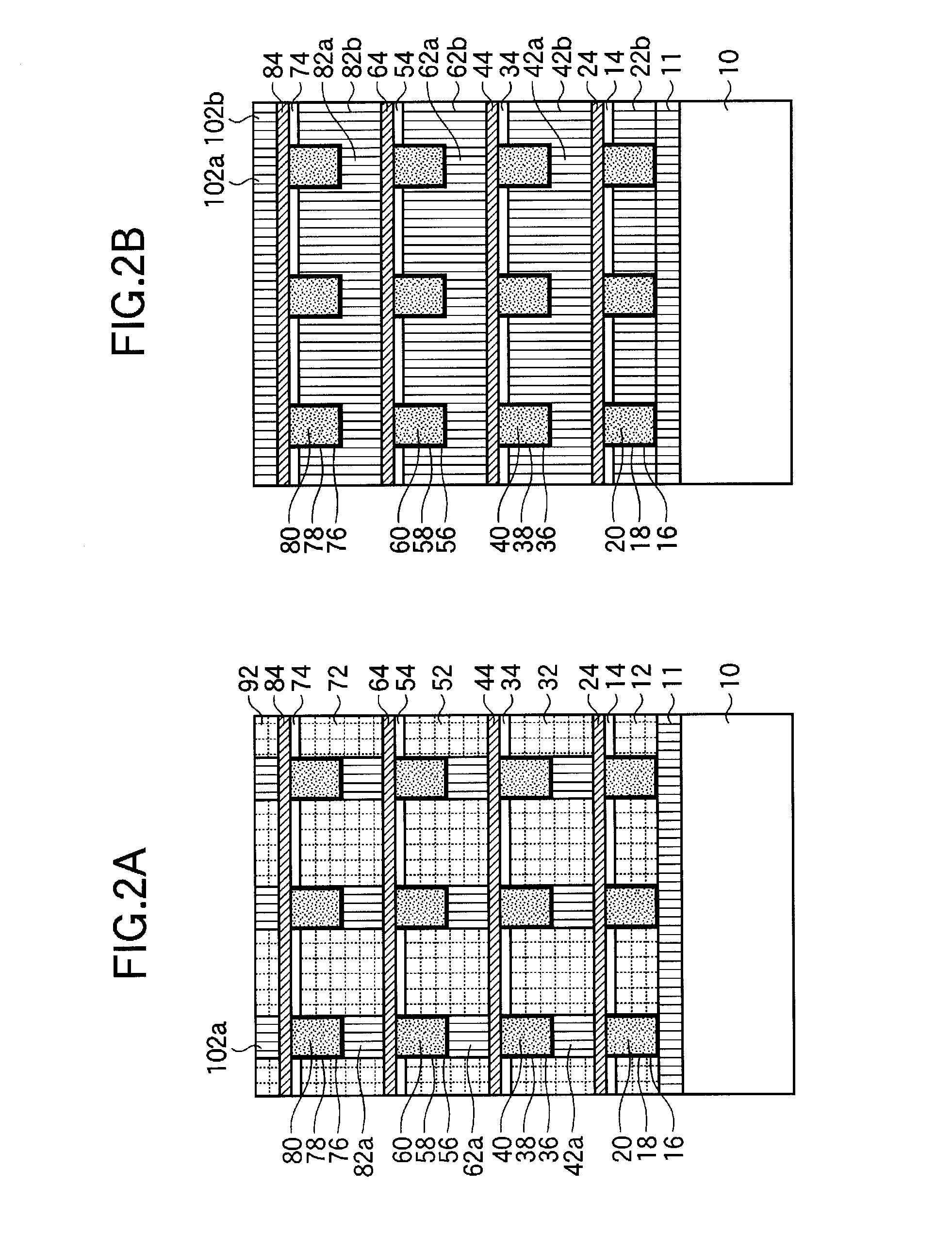
[0129]First, the method of manufacturing the semiconductor device according to an example 1 of this embodiment will be described. In this example, for example, the semiconductor device of the first basic configuration having the reinforcement insulating films 22b, 42b, 62b, 82b without overlapping with the wirings cannot be manufactured, but the semiconductor device of the fourth basic configuration can be manufactured at low cost.
[0130]FIGS. 35A to 39 are process cross-sectional views showing the method of manufacturing the semiconductor device according to this example. The illustration and description of a manufacturing process for a transistor and the like in a lower portion than the wiring are omitted. First, as shown in FIG. 35A, a SiO2 film 11 serving as an underlying insulating film is film-formed on the entire surface on a silicon substrate 10. Next, on the entire surface on the SiO2 film 11, for example, a SiOC film of a film thickness 250 nm is film-formed by a CVD method...
example 2
[0141]Next, a method of manufacturing the semiconductor device according to an example 2 of this embodiment will be described. In this example, the reinforcement insulating films 22b, 42b, 62b, 82b of the first basic configuration or the reinforcement insulating films absent immediately below or above the wirings of the reinforcement insulating films 22a, 42b, 62a, 82b and the like of the third basic configuration can be formed by adding a photo mask.
[0142]FIGS. 40A to 43 are process cross-sectional views showing the method of manufacturing the semiconductor device according to this example. First, on the entire surface of a silicon substrate 10 as shown in FIG. 40A, a SiO2 film 11 of a film thickness 150 nm, a silicon nitride film (SiN film) 132 of a film thickness 50 nm, a SiO2 film 134 of a film thickness 250 nm serving as a reinforcement insulating film, a SiC film 136 of a film thickness 50 nm serving as a middle etch stopper (MES) film, and a SiO2 film 138 of a film thickness ...
example 3
[0150]Next, a method of manufacturing a semiconductor device according to an example 3 of this embodiment will be described. The wiring 20 is formed after the low dielectric constant film 12 is formed in the example 2, whereas the low dielectric constant film 12 is formed after the wiring 20 is formed in this example.
[0151]FIGS. 44A to 46 are process cross-sectional views showing the method of manufacturing the semiconductor device according to this example. First, on the entire surface of a silicon substrate 10 as shown in FIG. 44A, a SiO2 film 11 of a film thickness 500 nm, a SiN film 132 of a film thickness 50 nm, a SiO2 film 134 of a film thickness 250 nm, a SiC film 136 of a film thickness 50 nm serving as an MES film, a SiO2 film 138 of a film thickness 250 nm, and a SiC film of a film thickness 50 nm serving as a hard mask film 14 all are film-formed in this order, for example, using a CVD method.
[0152]Next, as shown in FIG. 44B, a via hole 130 is formed by a photolithography...
PUM
 Abstract
Description
Claims
Application Information