Packaging substrate having electrical connection structure and method for fabricating the same

a technology of electrical connection and packaging substrate, which is applied in the direction of superimposed coating process, resistive material coating, liquid/solution decomposition chemical coating, etc., can solve the problem of poor uniform thickness and size of solder bumps, adversely affecting electrical connection quality, joint separation or breakage between solder bumps, etc. problem, to achieve the effect of less quality variance, uniform thickness and size, and reduced joint stress

Inactive Publication Date: 2011-06-07
UNIMICRON TECH CORP
View PDF9 Cites 6 Cited by
  • Summary
  • Abstract
  • Description
  • Claims
  • Application Information

AI Technical Summary

Benefits of technology

[0010]Another object of the present invention is to provide a packaging substrate having an electrical connection structure and a method for fabricating the same such that electroplated solder bumps formed on the surfaces of the conductive pads have a preferred uniformity in thickness and size, thereby improving the product reliability and providing better electrical connection quality.
[0019]Therefore, the electroplated solder bumps are formed in the openings of the solder mask layer, uniformly formed on the surface of the second conductive seed-layer and covering the conductive pads. Further, since the electroplated solder bumps have less quality variance, after a reflowing process applied thereto, the reflowed electroplated solder bumps are uniform in thickness and size. Further, the electroplated solder bumps with much larger height can reduce joint stress, thereby improving the electrical connection reliability of the electroplated solder bumps and meeting the fine-pitch requirement.

Problems solved by technology

In the above-described method, since the solder bumps 14 are filled in the openings 120 of he solder mask layer 12 and the openings 130 of the mold plate 13 by coating or printing, the quality of the solder bumps 14 is not easy to control, which can easily lead to poor uniformity in thickness and size of the solder bumps 14, thereby adversely affecting the electrical connection quality.
When temperature in a thermal recycling process of the fabrication process varies or the completed package is in use, the joint strength is not sufficient to endure the stress caused by a CTE difference between the chip and the substrate, thus 15 resulting in joint separation or breakage between the solder bumps 14′ and the electrode pads and failing to provide a preferred electrical connection.

Method used


Image

  • Packaging substrate having electrical connection structure and method for fabricating the same
  • Packaging substrate having electrical connection structure and method for fabricating the same
  • Packaging substrate having electrical connection structure and method for fabricating the same

Examples


first embodiment

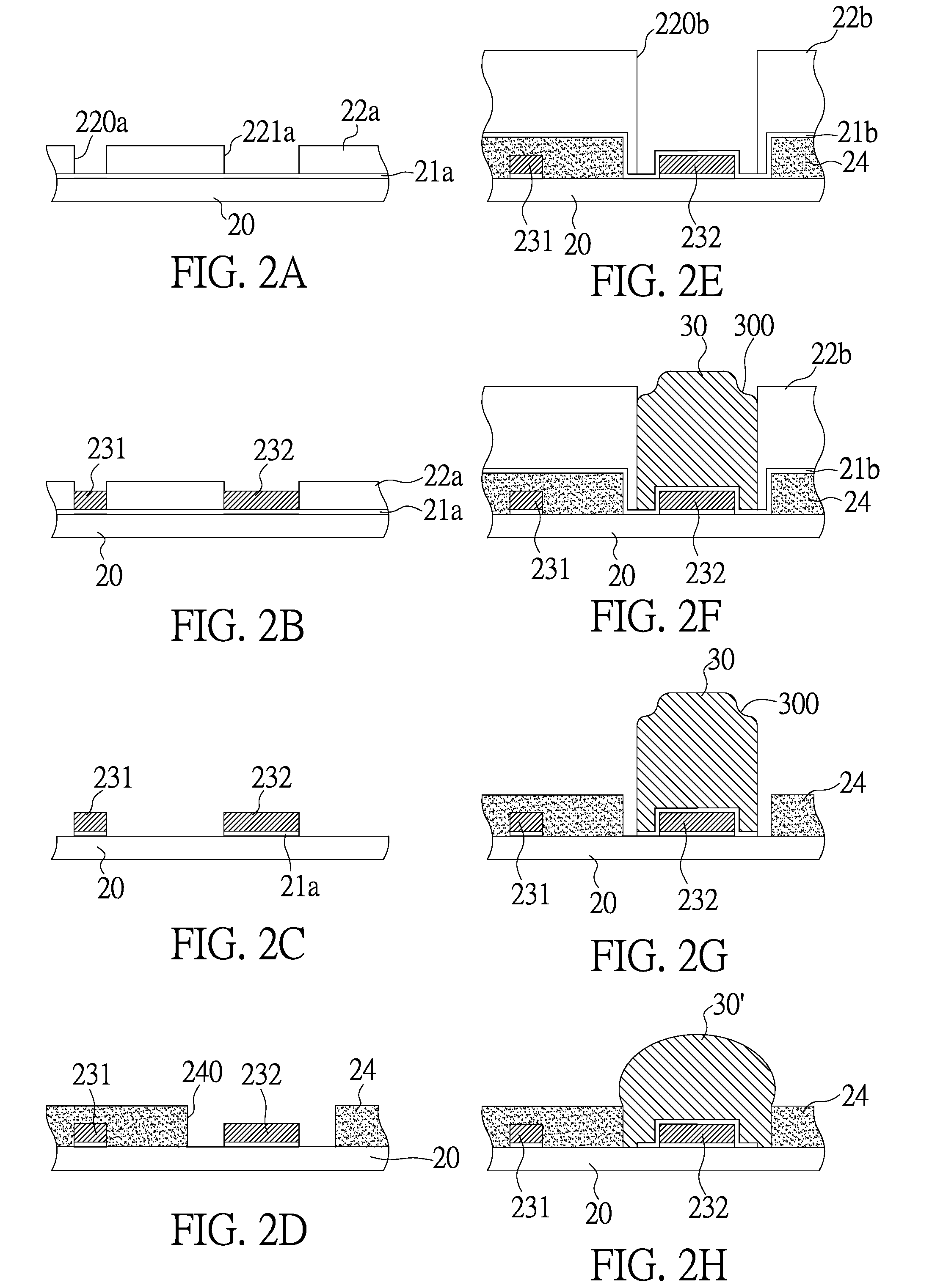
[0025]FIGS. 2A to 2H are sectional diagrams showing a method for fabricating a packaging substrate having an electrical connection structure according to a first embodiment of the present invention.

[0026]As shown in FIG. 2A, a substrate body 20 is provided, a first conductive seed-layer 21a is formed on a surface thereof and a patterned resist layer 22a is formed on the surface of the first conductive seed-layer 21a. The resist layer 22a has a plurality of openings 220a, 221a to expose a part of the first conductive seed-layer 21a.

[0027]As shown in FIG. 2B, through an electroplating process, circuit 231 is formed in the openings 220a of the first conductive seed-layer 21a and meanwhile conductive pads 232 are formed in the openings 221a. The circuit 231 and the conductive pads 232 can be made of copper.

[0028]As shown in FIG. 2C, the patterned resist layer 22a and the first conductive seed-layer 21a covered by the resist layer 22a are removed to expose the circuit 231 and the conduc...

second embodiment

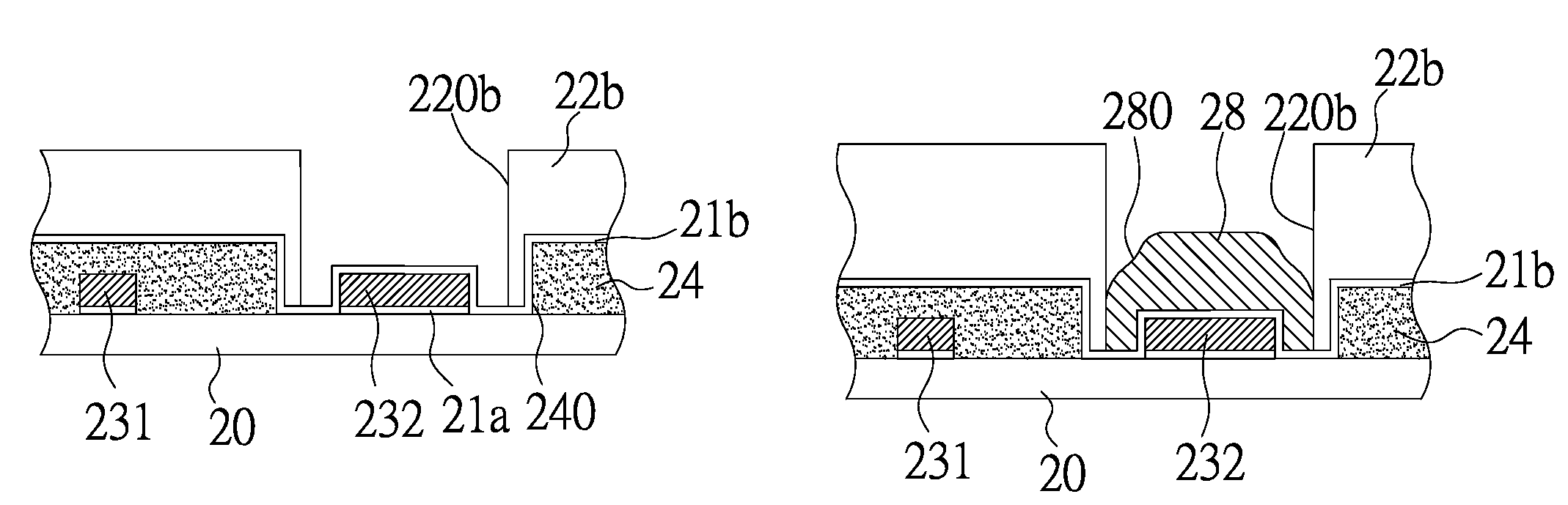
[0036]FIGS. 3A to 3E are sectional diagrams showing a method for fabricating a packaging substrate having an electrical connection structure according to a second embodiment of the present invention. A difference of the present embodiment from the first embodiment is metal bumps are formed between the conductive pads and the electroplated solder bumps.

[0037]As shown in FIG. 3A, a structure as shown in FIG. 2E is provided, a plurality of first openings 220b are formed in the first resist layer 22b to expose part of the second conductive seed-layer 21b, wherein each of the first openings 220b is larger in size than each of the conductive pads 232 and smaller in size than each of the openings 240 of the solder mask layer 24.

[0038]As shown in FIG. 3B, metal bumps 28 are formed in the first openings 220b through the second conductive seed-layer 21b by electroplating to completely enclose the conductive pads 232. The metal bumps 28 can protrude above the surface of the 25 solder mask laye...

third embodiment

[0045]FIGS. 4A to 4E are sectional diagrams showing a method for fabricating a packaging substrate having an electrical connection structure according to a third embodiment of the present invention. A difference of the present embodiment from the above-described embodiments is a metal attachment layer is formed between the conductive pads and the electroplated solder bumps.

[0046]As shown in FIG. 4A, a structure as shown in FIG. 2D is provided, a metal attachment layer 26 is formed on the surfaces of the conductive pads 232 by chemical deposition or physical deposition and covering the conductive pads 232. The metal attachment layer 26 can be made of one of Ni, Ni / Au, Zn, and Ni / Pd / Au.

[0047]As shown in FIG. 4B, a second conductive seed-layer 21b is formed on the surface of the solder mask layer 24, the inner walls of the openings 240 and a surface of the metal attachment layer 26. A first resist layer 22b is formed on a surface of the second conductive seed-layer 21b and a plurality ...


PUM

PropertyMeasurementUnit
sizeaaaaaaaaaa
conductiveaaaaaaaaaa
thicknessaaaaaaaaaa

Abstract

A packaging substrate having an electrical connection structure and a method for fabricating the same are provided. The packaging substrate have a substrate body with a plurality of conductive pads on a surface thereof; a solder mask layer disposed on the substrate body with a plurality of openings corresponding to the conductive pads, the size of each of the openings being larger than each of the conductive pads; and electroplated solder bumps for covering the conductive pads to provide better bond strength and reliability.

Description

BACKGROUND OF THE INVENTION[0001]1. Field of the Invention[0002]The present invention relates generally to packaging substrates having an electrical connection structure and methods for fabricating the same, and more particularly to, a packaging substrate having an electrical connection structure for electrically connecting a chip and a method for fabricating the same.[0003]2. Description of Related Art[0004]The current flip chip technique involves electrically connecting a semiconductor chip to a packaging substrate, wherein the semiconductor chip has a plurality of electrode pads on an active surface thereof, and the packaging substrate has a plurality of conductive pads corresponding to the electrode pad. A solder structure or other conductive adhesive material is disposed between the electrode pads and the corresponding conductive pads for providing electrical connection and mechanical connection between the semiconductor chip and the packaging substrate.[0005]Referring to FIGS....

Claims


Application Information

Patent Timeline
Patent Type & Authority Patents(United States)
IPC IPC(8): H01L23/48
CPCH01L21/4853H05K3/3473H01L23/49816Y10T428/24331H05K3/244H05K3/3452H05K3/4007H05K2201/0367H05K2201/0989H05K2203/043H05K2203/054H01L2224/05563H01L2224/05571H01L2224/13022H01L2224/13109H01L2224/13006H01L2924/01327H01L2924/0002H01L2224/0401H01L2924/00H01L2224/05552
Inventor HSU, SHIH-PING
Owner UNIMICRON TECH CORP
Why Eureka
Try Eureka