Process of grounding heat spreader/stiffener to a flip chip package using solder and film adhesive

a technology of heat spreader/stiffener and flip chip, applied in the direction of semiconductor devices, semiconductor/solid-state device details, electrical apparatus, etc., can solve the problems of additional manufacturing steps, handling problems, and high cost of conventional techniques, so as to reduce or eliminate the manufacturing steps of printed circuit boards, reduce the cost, and reduce the effect of handling problems

Active Publication Date: 2011-06-28
BELL SEMICON LLC
View PDF14 Cites 18 Cited by
  • Summary
  • Abstract
  • Description
  • Claims
  • Application Information

AI Technical Summary

Benefits of technology

[0004]The objects, features and advantages of the present invention include providing a method and / or architecture for grounding a heat spreader / stiffener to a flip chip package using solder and film adhesive that may (i) provide shielding that is transparent to an end user, (ii) reduce cost, (iii) reduce or eliminate manufacturing steps for printed circuit boards, (iv) reduce or eliminate handling problems, (v) integrate electromagnetic shielding into the integrated circuit package and / or (vi) provide higher reliability than epoxy attachment.

Problems solved by technology

The conventional technique is costly, involves additional manufacturing steps for the PCB, and has handling problems.

Method used


Image

  • Process of grounding heat spreader/stiffener to a flip chip package using solder and film adhesive
  • Process of grounding heat spreader/stiffener to a flip chip package using solder and film adhesive
  • Process of grounding heat spreader/stiffener to a flip chip package using solder and film adhesive

Examples


Embodiment Construction

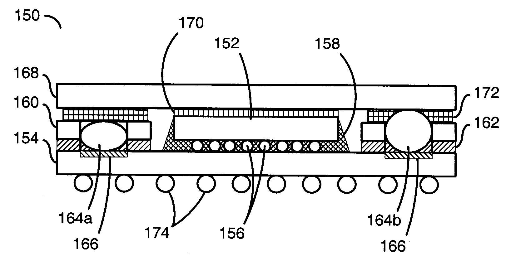
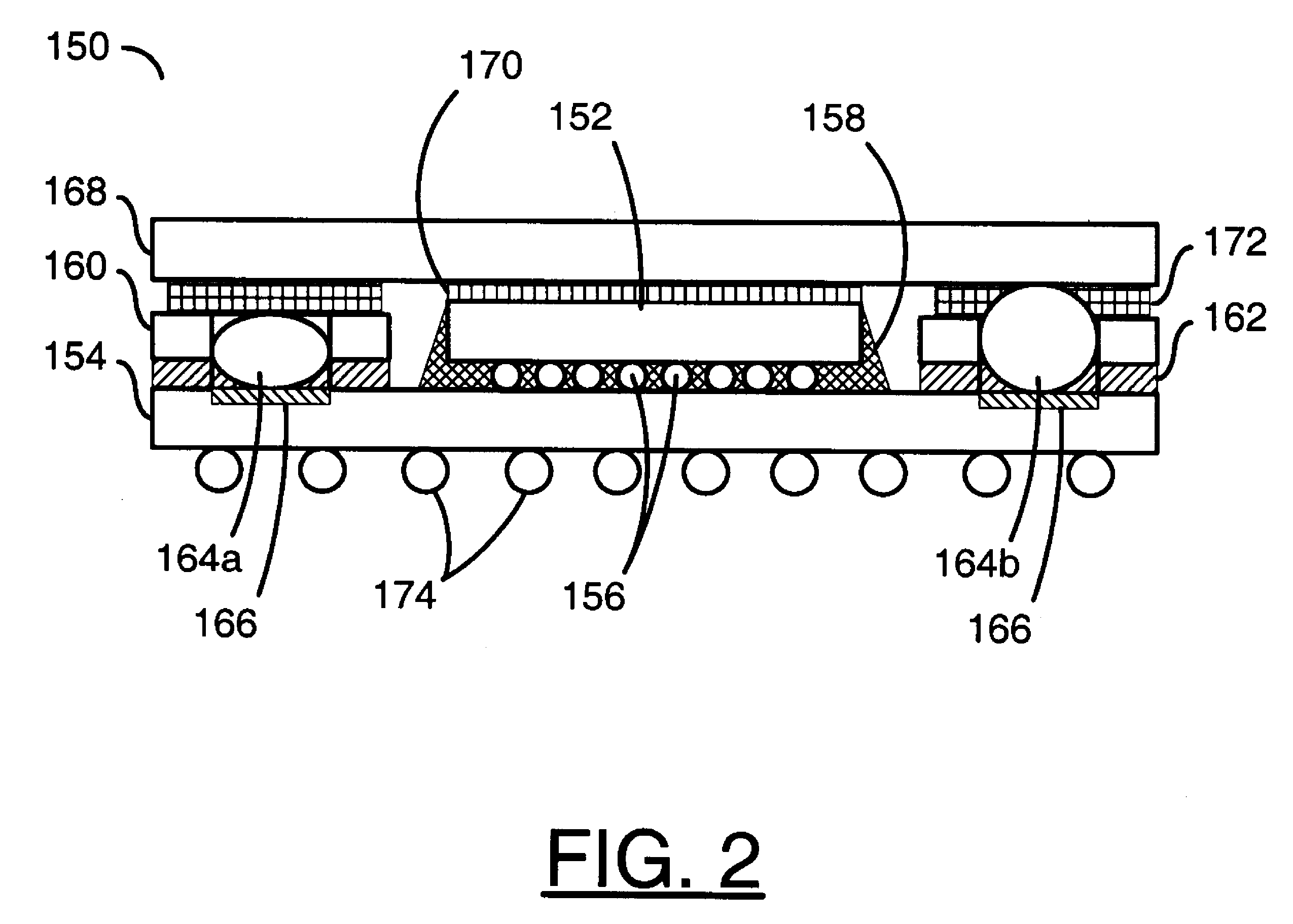
[0009]The present invention generally provides a process and architecture for grounding a heat spreader / stiffener to a flip chip package. Flip chip packages may be identified by manufacturers using designations such as FPBGA, FCPBGA, FCBGA, etc. The present invention generally provides a process for integrating electromagnetic shielding into the package by grounding the heat spreader / stiffener through the package substrate. In one example, a combination of film adhesive and solder may be used to mechanically and electrically connect the heat spreader / stiffener to the package substrate. The shielding provided by the present invention may be transparent to the customer (or end user). The present invention generally eliminates deficiencies of the conventional approach.

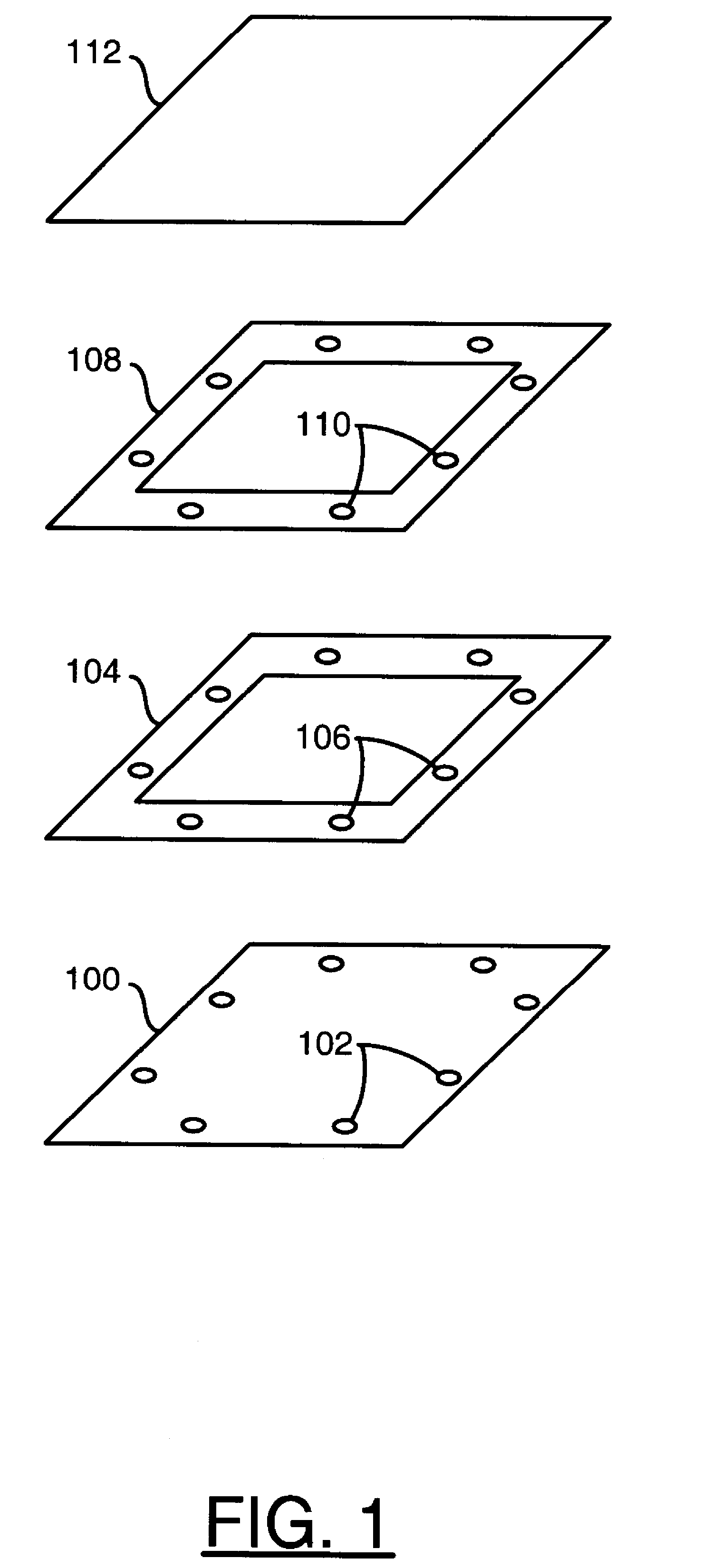
[0010]Referring to FIG. 1, a diagram is shown illustrating attachment of a heat spreader / stiffener to a package substrate in accordance with the present invention. In one example, a substrate 100 may be implemented with a...


PUM


Abstract

A method of grounding a heat spreader / stiffener to a flip chip package comprising the steps of attaching an adhesive film to a substrate and attaching a stiffener to the adhesive film. The adhesive film may have a number of first holes corresponding with a number of grounding pads on the substrate. The grounding pads may be configured to provide electrical grounding. The stiffener may have a number of second holes corresponding with the number of first holes of the adhesive film and number the grounding pads of the substrate. The grounding pads are generally exposed through the first and the second holes.

Description

FIELD OF THE INVENTION[0001]The present invention relates to semiconductor chip assembly generally and, more particularly, to a method and / or architecture for grounding a heat spreader / stiffener to a flip chip package using solder and film adhesive.BACKGROUND OF THE INVENTION[0002]Conventional package grounding for electromagnetic shielding is done via a heat sink and / or heat spreader. The heat sink and / or heat spreader are connected to a printed circuit board (PCB) using clamps, wires, or some other connecting means. The conventional technique is costly, involves additional manufacturing steps for the PCB, and has handling problems.SUMMARY OF THE INVENTION[0003]The present invention concerns a method of grounding a heat spreader / stiffener to a flip chip package comprising the steps of attaching an adhesive film to a substrate and attaching a stiffener to the adhesive film. The adhesive film may have a number of first holes corresponding with a number of grounding pads on the substr...

Claims


Application Information

Patent Timeline
Patent Type & Authority Patents(United States)
IPC IPC(8): H01L23/10H01L23/34
CPCH01L23/10H01L23/36H01L23/49833H01L23/50H01L23/552H01L2224/73253H01L2224/73204H01L2224/32225H01L2224/16225H01L2924/3025H01L2924/15311H01L2924/1517H01L2924/15153H01L24/16H01L2224/16H01L2924/01057H01L2924/01079H01L2924/14H01L2924/00H01L2924/16195
Inventor CELIK, ZEKI Z.KUTLU, ZAFER S.SHAH, VISHAL
Owner BELL SEMICON LLC
Why Eureka
Try Eureka