Semiconductor package having improved heat spreading performance

a technology of semiconductors and heat dissipation, applied in the direction of semiconductor devices, semiconductor/solid-state device details, electrical apparatus, etc., can solve the problems of affecting the reliability of the internal chips and the package as a whole, limiting the amount of heat that can be radiated, and high packaging temperature, so as to achieve the effect of spreading the heat produced in the interior

Inactive Publication Date: 2011-07-05
SAMSUNG ELECTRONICS CO LTD
View PDF10 Cites 2 Cited by
  • Summary
  • Abstract
  • Description
  • Claims
  • Application Information

AI Technical Summary

Benefits of technology

[0013]Embodiments of the present invention provide a semiconductor package having a structure that can effectively spread heat produced in the interior of the package.

Problems solved by technology

This leads to higher temperatures in the packages, especially for multi chip packages (MCPs), which contain two or more chips in one package.
High temperatures in the interior of a package can cause stress on the chips mounted in the package and often result in malfunctions.
However, multi-chip semiconductor packages such as dual stack packages (DSPs) or quad stack packages (QSPs) produce a great amount of heat, but there is a limit to the amount of heat that can be radiated.
Further, there is a problem in that internal chips of a multi-chip package may reach different temperatures, which may affect the reliability of the internal chips and the package as a whole.

Method used


Image

  • Semiconductor package having improved heat spreading performance
  • Semiconductor package having improved heat spreading performance
  • Semiconductor package having improved heat spreading performance

Examples


Embodiment Construction

[0024]The present invention will now be described more fully hereinafter with reference to the accompanying drawings, in which exemplary embodiments of the invention are shown. Like numbers refer to like elements throughout the specification.

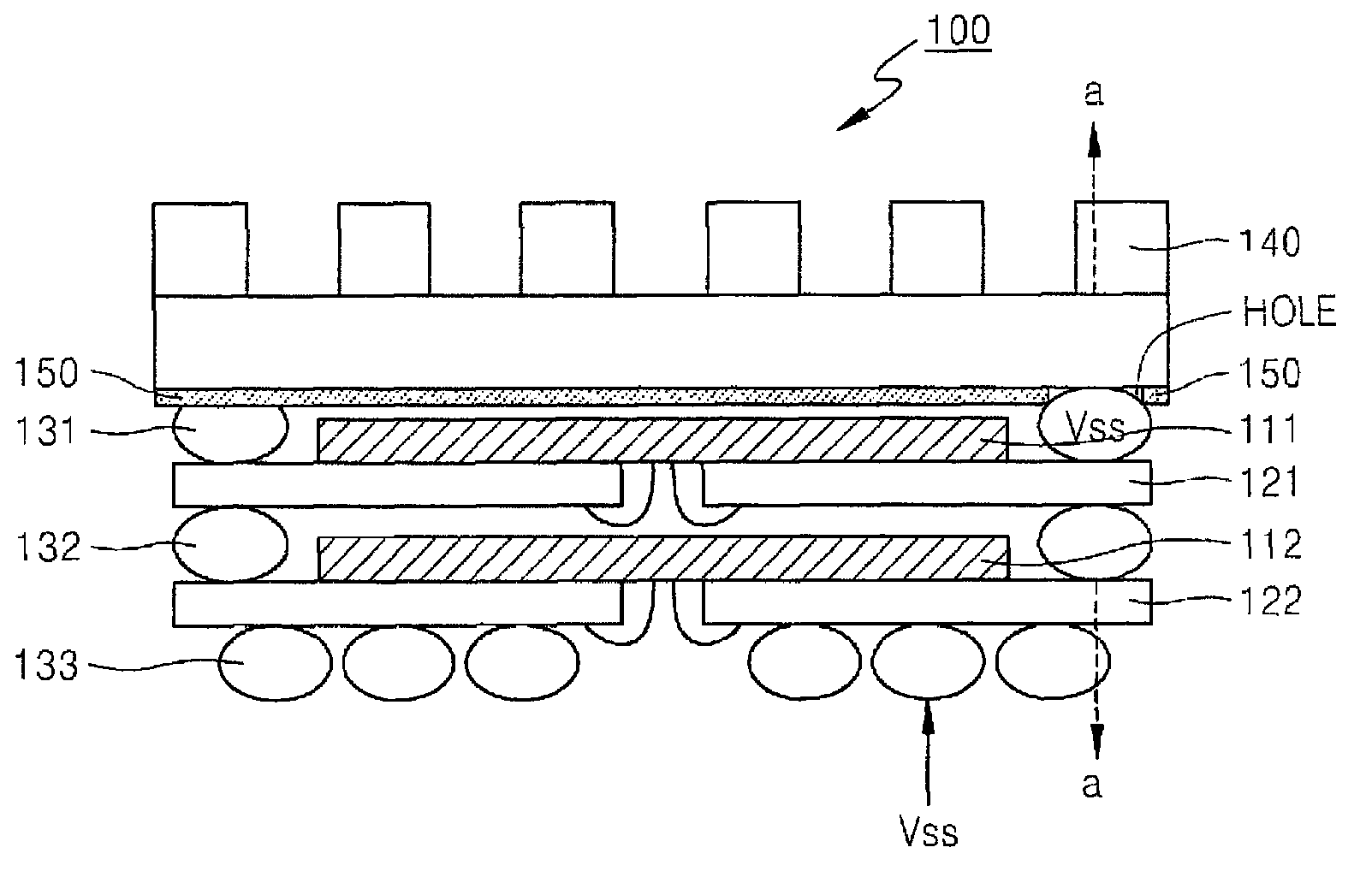
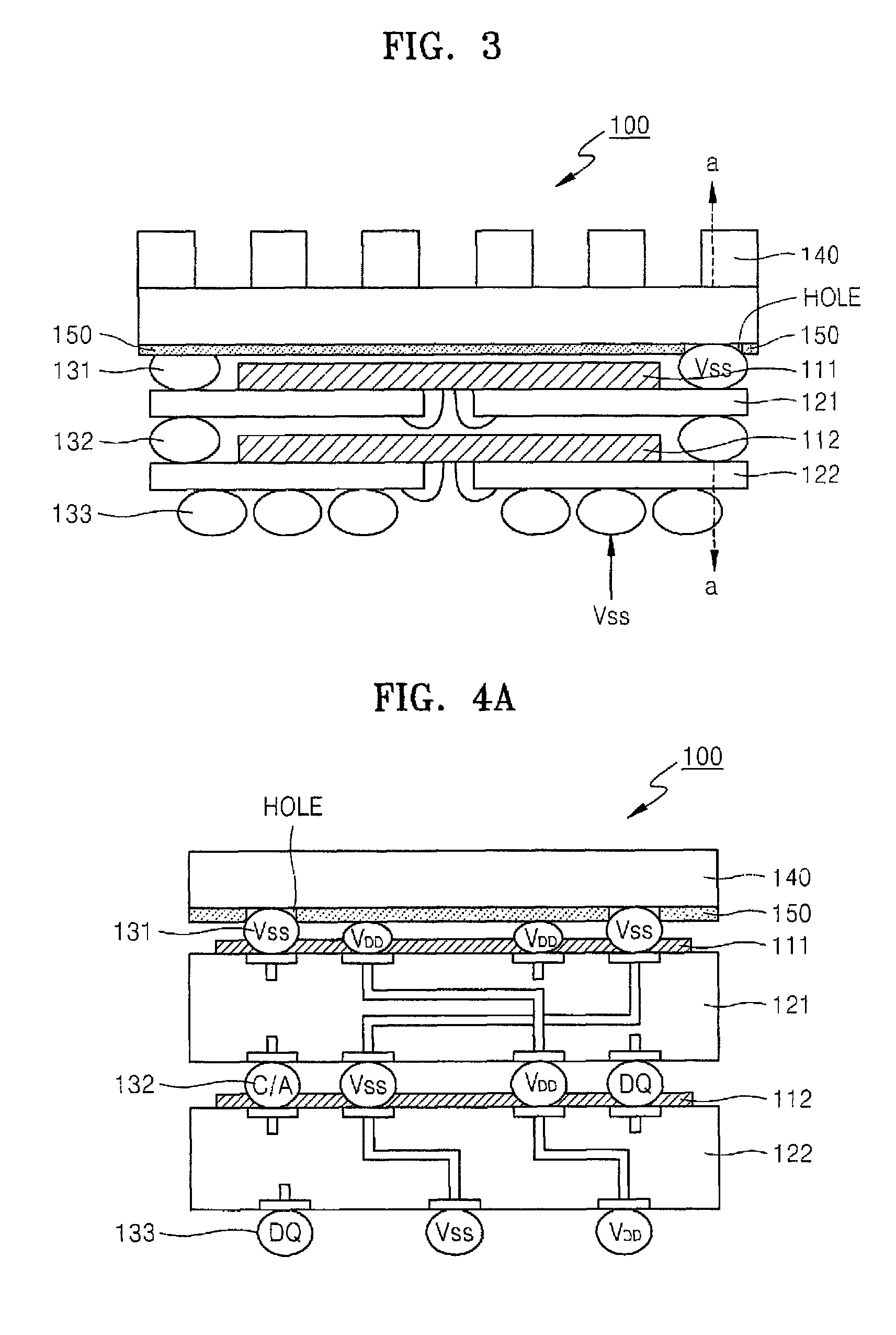
[0025]FIG. 3 is a sectional view of a semiconductor package according to an embodiment of the present invention. As shown in this figure, the semiconductor package 100 may include one or more semiconductor chips 111 and 112, one or more substrates (PCBs) 121 and 122, and a plurality of solder balls 131, 132, and 133.

[0026]In the semiconductor package 100 according to an embodiment of the present invention, one or more semiconductor chips may be arranged in a stack structure. As an example, semiconductor packages provided with a multi-chip structure, such as a dual stack package (DSP) and a quad stack package (QSP), may be applied. The semiconductor package shown in FIG. 3 includes two stacked semiconductor chips 111 and 112, as an example of a m...


PUM


Abstract

A semiconductor package having a structure in which heat produced in the interior of the package is effectively spread to the outside of the package is provided. The semiconductor package includes one or more semiconductor chips, one or more substrates (PCBs) having the semiconductor chips respectively attached thereto, a plurality of conductive balls such as a plurality of solder balls to provide voltages and signals to the one or more semiconductor chips, and a heat sink positioned to spread heat produced in the interior of the package to the outside and directly connected to at least one of the plurality of solder balls.

Description

CROSS-REFERENCE TO RELATED PATENT APPLICATION[0001]This application claims the benefit of Korean Patent Application No. 10-2006-0113408, filed on Nov. 16, 2006, in the Korean Intellectual Property Office, the disclosure of which is incorporated herein by reference.BACKGROUND[0002]1. Field of the Invention[0003]The present invention relates to a semiconductor package, and more particularly, to a semiconductor package capable of effectively radiating heat produced in the interior thereof.[0004]2. Description of the Related Art[0005]As semiconductor packages having semiconductor chips mounted therein are highly integrated and operated at high speeds, their operation speeds have been greatly increased and their sizes have been reduced. This leads to higher temperatures in the packages, especially for multi chip packages (MCPs), which contain two or more chips in one package. High temperatures in the interior of a package can cause stress on the chips mounted in the package and often res...

Claims


Application Information

Patent Timeline
Patent Type & Authority Patents(United States)
IPC IPC(8): H01L23/373
CPCH01L25/0657H01L23/13H01L23/367H01L2224/16H01L2224/4824H01L2225/0651H01L2225/06572H01L2225/06586H01L2225/06589H01L2924/15311H01L2224/32225H01L2224/73204H01L2924/15331H01L2225/0652H01L2924/00014H01L2924/00011H01L2224/0401H01L23/36H01L23/12
Inventor PAEK, SOO-JINKIM, WOO-SEOPKIM, KI-SUNG
Owner SAMSUNG ELECTRONICS CO LTD
Why Eureka
Try Eureka