Method of manufacturing wiring board, method of manufacturing light emitting device using the wiring board, wiring board, and light emitting device using the wiring board

Active Publication Date: 2017-12-14
NICHIA CORP
View PDF10 Cites 3 Cited by
  • Summary
  • Abstract
  • Description
  • Claims
  • Application Information

AI Technical Summary

Benefits of technology

[0009]Thus, a less costly method of manufacturing a wiring board for mounting a semiconductor element that consumes great power such as a light emitting element; a method of manufacturing a ligh

Problems solved by technology

Treatments of such waste liquids lead t

Method used


Image

  • Method of manufacturing wiring board, method of manufacturing light emitting device using the wiring board, wiring board, and light emitting device using the wiring board
  • Method of manufacturing wiring board, method of manufacturing light emitting device using the wiring board, wiring board, and light emitting device using the wiring board
  • Method of manufacturing wiring board, method of manufacturing light emitting device using the wiring board, wiring board, and light emitting device using the wiring board

Examples


first embodiment

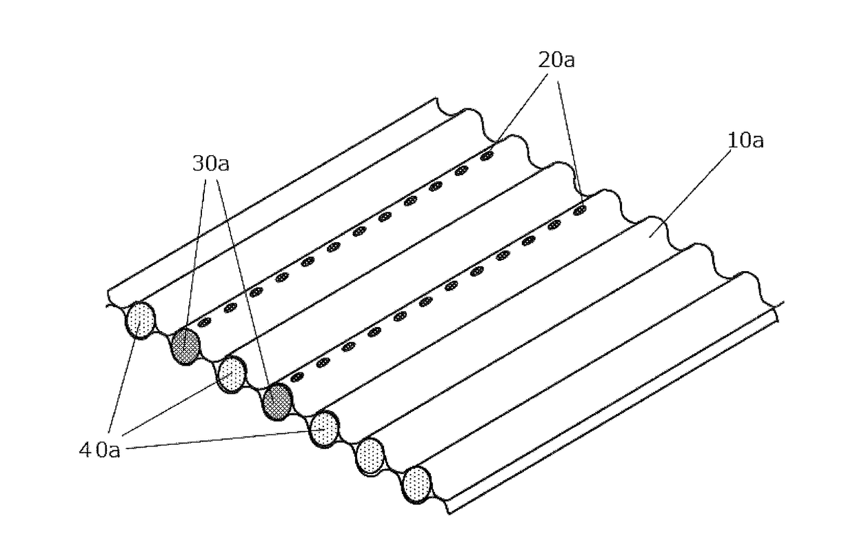
[0029]FIGS. 1 to 5 are schematic diagrams showing steps of manufacturing a wiring board 100 according to the present embodiment. FIG. 6 is a schematic diagram of the wiring board 100. The method of manufacturing a wiring board according to the present embodiment includes: providing at least one first conductive member; covering with an insulating member; disposing at least one second conductive member; and cutting.

Providing First Conductive Members

[0030]In providing one or more first conductive members, for example as shown in FIG. 1, a plurality of first conductive members 30a having a cylindrical columnar shape are provided. In the present embodiment, one or more spacer members 40a being similar in shape to the first conductive members are also provided in addition to the first conductive members 30a. In the present embodiment, the surface of each spacer member 40a is electrically insulated. Subsequently, for example, the first conductive members 30a and the spacer members 40a are...

second embodiment

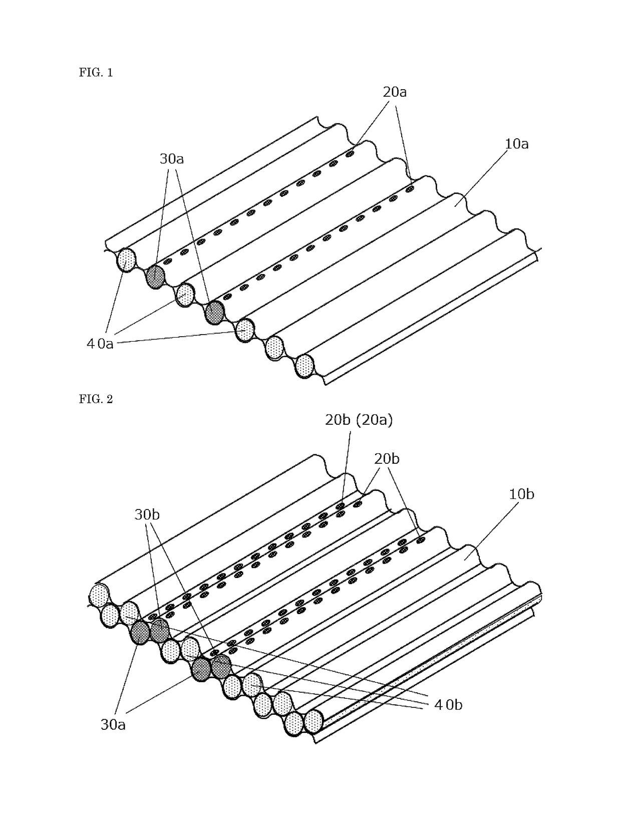
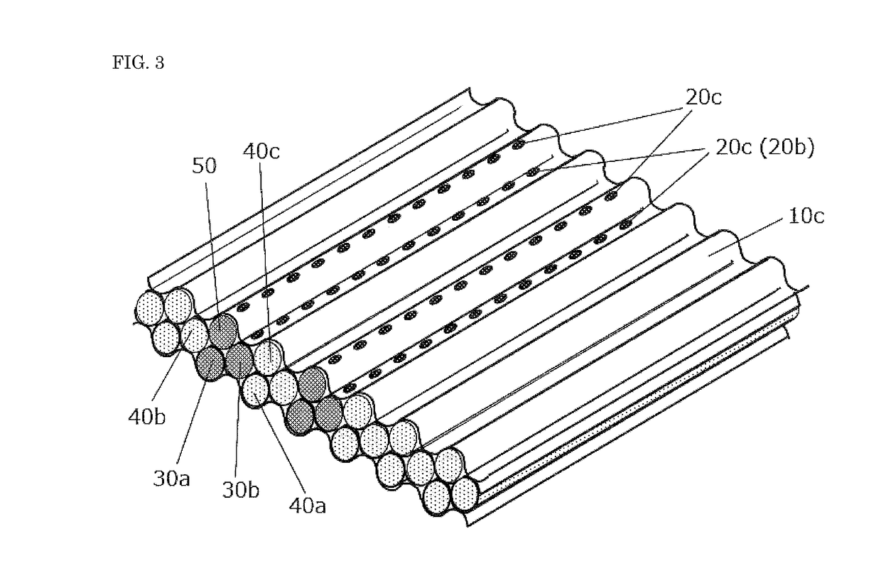
[0049]In a second embodiment, the first conductive members 30a and the second conductive members 50 are respectively layered on each other having the insulating member 10a provided with the openings 20a interposed therebetween, as shown in FIGS. 8 to 13. The second embodiment can be achieved by the same steps as the first embodiment except that the spacer members 40a, 40b, 40c are identical to the conductive members in material and shape.

[0050]According to the present embodiment, since the spacer members are conductive, a wiring board can have low electrical resistance and improved heat dissipation property.

third embodiment

[0051]In a third embodiment, as shown in FIGS. 14A and 14B, as part of the conductive members forming a wiring, conductive members each being a round tube and / or a resin core provided with a metal layer on its outer side are disposed, to obtain a wiring board similarly to the first embodiment. In this manner, a reduction in weight is achieved. FIG. 14A is a perspective view of the wiring board according to the present embodiment. FIG. 14B is a cross-sectional view taken along line A-A′ in FIG. 14A. By cutting the conductive members each including a resin core 32 provided with a metal layer 34 on the outer side of its lateral surface, resin core conductive bodies 132 can be obtained. By cutting the round tubes, through hole-including conductive bodies 134 are obtained. In the present embodiment, conductive joining members 136 made of solder or the like are respectively disposed on the openings provided on the sheet-like insulating member 10, therefore the conductive members are elect...


PUM


Abstract

A method of manufacturing a wiring board according to one embodiment of the present disclosure includes: providing at least one first conductive member that serves as part of a wiring; covering the at least one first conductive member with an insulating member that has at least one opening; disposing at least one second conductive member on the opening of the insulating member, the second conductive member serving as part of the wiring; electrically joining the at least one first conductive member and the at least one second conductive member to each other at the opening; and cutting a region including the at least one first conductive member, the insulating member, and the at least one second conductive member, to form an element mounting surface.

Description

CROSS-REFERENCE TO RELATED APPLICATION[0001]This application claims priority to Japanese Patent Application No. 2016-101765, filed on May 20, 2016, the disclosure of which is hereby incorporated by reference in its entirety.BACKGROUNDField of the Invention[0002]The present disclosure relates to a method of manufacturing a wiring board, a method of manufacturing a light emitting device using the wiring board, a wiring board, and a light emitting device using the wiring board.Discussion of the Background[0003]As printed wiring boards (PWBs) used for mounting semiconductor elements, various kinds of wiring boards are known, such as an aluminum-based single-sided board, and a CEM-3 copper clad board. For example, Japanese Unexamined Patent Publication No. 2016-4770 discloses a method of manufacturing a light source mounting wiring board in which a wiring pattern is formed by partially removing layered copper foil by etching.SUMMARY[0004]However, such a conventional PWB using copper foil...

Claims


Application Information

Patent Timeline
IPC IPC(8): H01L33/64H01L33/62
CPCH01L33/647H01L2933/0075H01L2933/0066H01L33/62H01L25/0753H01L33/644H05K1/0204H05K3/4602H05K2201/10106H05K2203/0235
Inventor MARUTANI, YUKITOSHI
Owner NICHIA CORP
Why Eureka
Try Eureka