Method of manufacturing nonvolatile memory device
a nonvolatile memory and manufacturing method technology, applied in the direction of semiconductor devices, basic electric elements, electrical appliances, etc., can solve the problems of deterioration of leakage current and reliability characteristics, uniform distribution of cell threshold voltage (vsub>th/sub>), and reduction of thickness at both edges of ono layers. , to achieve the effect of suppressing a charge sharing phenomenon, improving retention characteristics, and improving film quality of nitride layers
- Summary
- Abstract
- Description
- Claims
- Application Information
AI Technical Summary
Benefits of technology
Problems solved by technology
Method used
Image
Examples
first embodiment
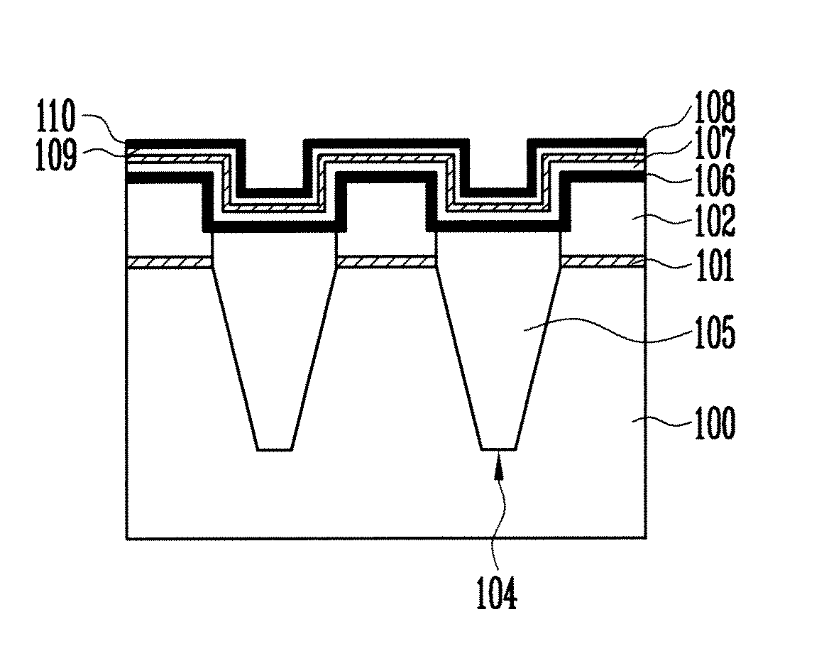
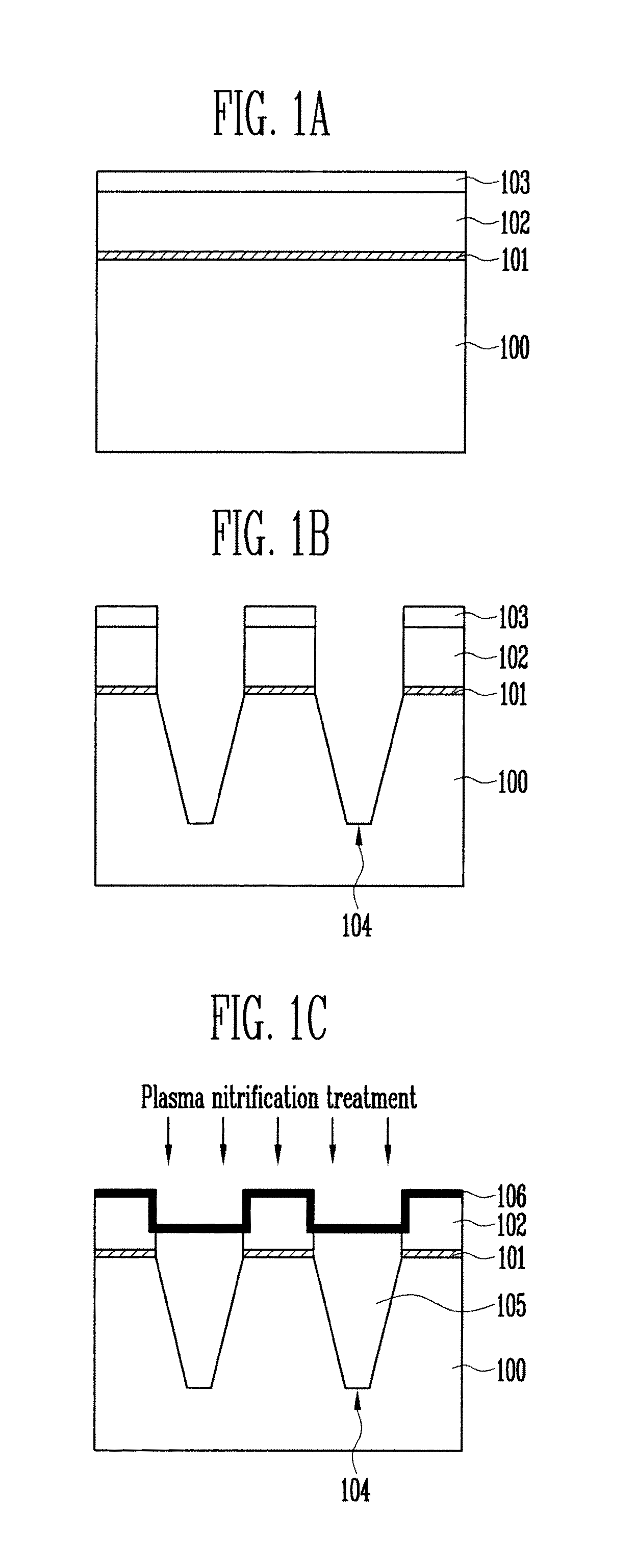
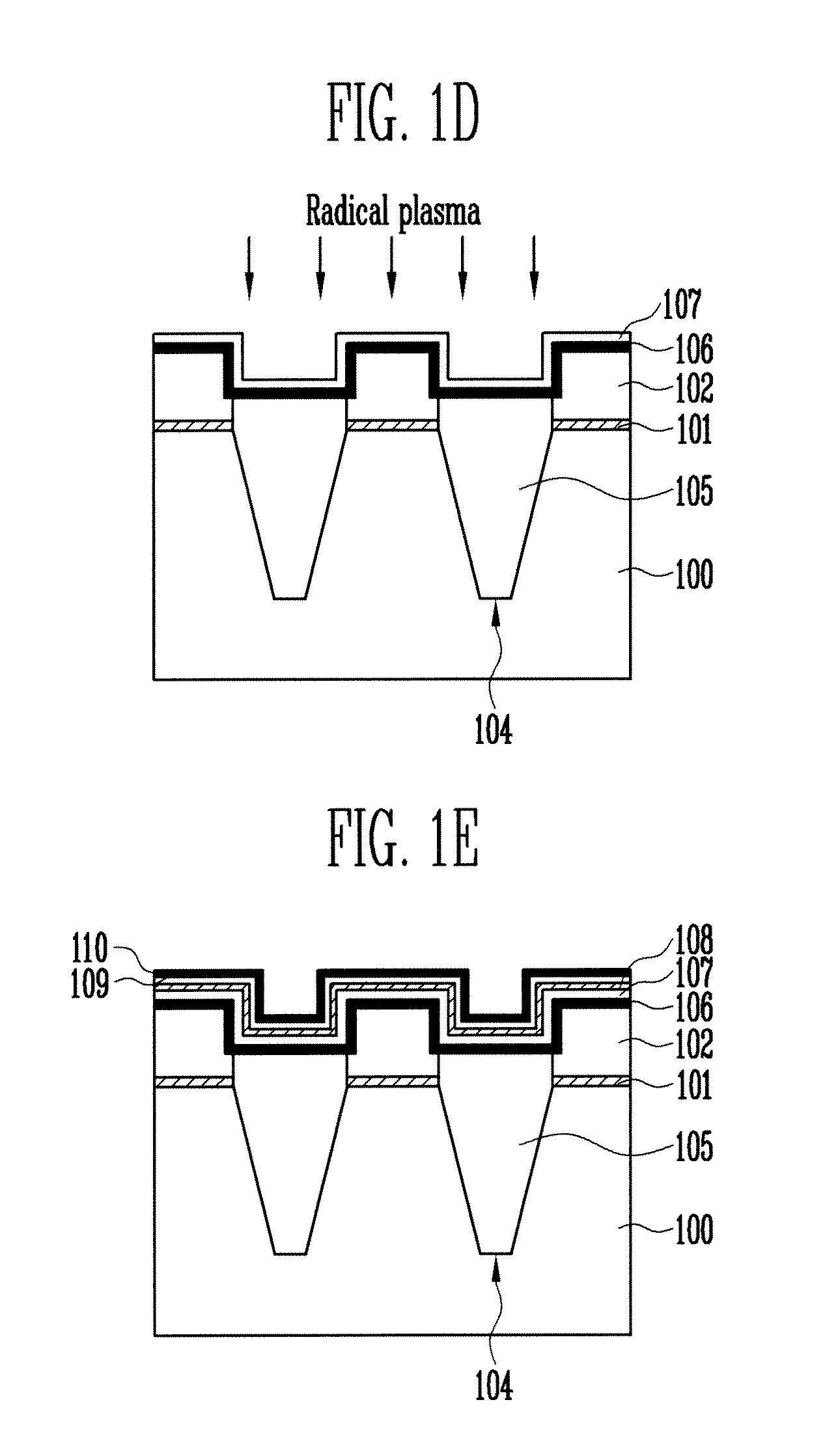
[0037]FIGS. 1A to 1E are cross-sectional views showing a method of manufacturing a nonvolatile memory device according to a
[0038]Referring to FIG. 1A, a tunnel insulating layer 101, a charge trap layer 102, and a hard mask layer 103 are sequentially formed over a semiconductor substrate 100. The tunnel insulating layer 101 preferably is formed of an oxide layer. The charge trap layer 102 preferably is formed of a polysilicon layer, or a nitride layer capable of trapping charges. In the case where the charge trap layer 102 is formed of a polysilicon layer, the charge trap layer 102 preferably comprises a dual layer, having an amorphous polysilicon layer not including impurities and a polysilicon layer including impurities. The hard mask layer 103 preferably has a dual structure of an oxide layer and a nitride layer.
[0039]Referring to FIG. 1B, a first etch process is performed to pattern the hard mask layer 103. A second etch process using the patterned hard mask layer 103 as an etch ...
second embodiment
[0064]FIGS. 6A to 6E are cross-sectional views illustrating a method of manufacturing a nonvolatile memory device according to a
[0065]Referring to FIG. 6A, a tunnel insulating layer 601, a charge trap layer 602, a buffer layer 603, a pad layer 604, and a hard mask layer 605 are sequentially formed over a semiconductor substrate 600. The tunnel insulating layer 601 preferably is formed of an oxide layer. The charge trap layer 602 preferably is formed of a polysilicon layer or a nitride layer capable of trapping charges. In the case where the charge trap layer 602 is formed of a polysilicon layer, the charge trap layer 602 preferably is formed to have a dual layer having an amorphous polysilicon layer not including impurities and a polysilicon layer including impurities. The buffer layer 603 preferably is formed of an oxide layer. The pad layer 604 preferably is formed of a nitride layer. The hard mask layer 605 can be formed to have a dual structure of an oxide layer and a nitride la...
third embodiment
[0080]FIGS. 8A to 8E are cross-sectional views showing a method of manufacturing a nonvolatile memory device according to a
[0081]Referring to FIG. 8A, a tunnel insulating layer 801, a charge trap layer 802, and a hard mask layer 803 are sequentially formed over a semiconductor substrate 800. The tunnel insulating layer 801 preferably is formed of an oxide layer. The charge trap layer 802 preferably is formed of a polysilicon layer or a nitride layer capable of trapping charges. In the case where the charge trap layer 802 is formed of a polysilicon layer, the charge trap layer 802 preferably comprises a dual layer, having an amorphous polysilicon layer not including impurities and a polysilicon layer including impurities. The hard mask layer 803 preferably is formed to have a dual structure of an oxide layer and a nitride layer.
[0082]Referring to FIG. 8B, a first etch process is performed to pattern the hard mask layer 803. A second etch process using the patterned hard mask layer 80...
PUM
 Abstract
Description
Claims
Application Information


