Method of Manufacturing Nonvolatile Memory Device

a nonvolatile memory and manufacturing method technology, applied in the direction of semiconductor devices, basic electric elements, electrical appliances, etc., can solve the problems of deterioration of leakage current and reliability characteristics, uniform distribution of cell threshold voltage (vsub>th/sub>), and reduction of thickness at both edges of ono layers. , to achieve the effect of suppressing a charge sharing phenomenon, improving retention characteristics, and improving film quality of nitride layers

Inactive Publication Date: 2010-11-25
SK HYNIX INC
View PDF6 Cites 15 Cited by
  • Summary
  • Abstract
  • Description
  • Claims
  • Application Information

AI Technical Summary

Benefits of technology

[0006]One embodiment relates to a method of manufacturing a nonvolatile memory device, in which a nitride layer and a first oxide layer, which forms a dielectric layer having an ONO structure, are formed over floating gates and isolation layers, and a radical plasma process is performed to improve the film quality of the nitride layer, thereby suppressing a charge sharing phenomenon and improving a retention characteristic. Further, after the ONO dielectric layer is formed, another nitride layer is formed on the ONO dielectric layer, thus making it possible to suppress a smile phenomenon of the ONO dielectric layer, and make the threshold voltage distributions of cells more uniform.
[0007]Another of the embodiments relates to a method of manufacturing a nonvolatile memory device, wherein, after isolation layers are formed, a selective nitrification process is performed to form a nitride layer on only a top surface and sidewalls of a conductive layer for floating gates that is formed in an active region of a semiconductor substrate, thereby being capable of preventing charges, which are trapped in the floating gates, from moving to neighboring gates when the memory device operates, and so improving the distribution and retention characteristics of the memory device.
[0009]Preferably, the radical plasma process is performed to increase the density of the first oxide layer and to improve the film quality of the first oxide layer.
[0022]After forming the dielectric layer, a radical plasma process preferably is performed to increase the density of the dielectric layer and to improve the film quality thereof.
[0023]After forming the passivation layer, a radical plasma process preferably is performed to increase the density of the passivation layer and the dielectric layer and to improve the film quality.

Problems solved by technology

Thus, the leakage current and a reliability characteristic are deteriorated, and a thickness at both edges of the ONO layer is reduced.
Further, there is a problem in that the uniformity of a cell threshold voltage (Vth) distribution deteriorates.

Method used


Image

  • Method of Manufacturing Nonvolatile Memory Device
  • Method of Manufacturing Nonvolatile Memory Device
  • Method of Manufacturing Nonvolatile Memory Device

Examples


first embodiment

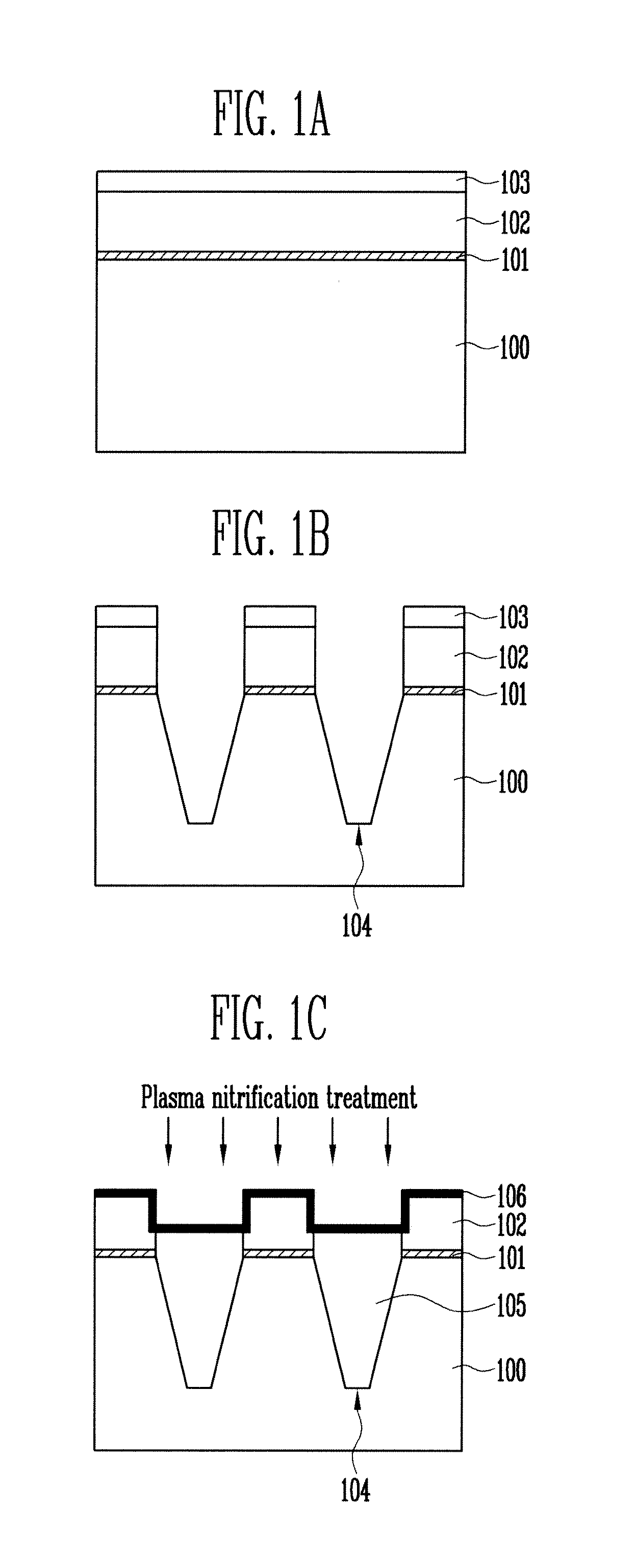
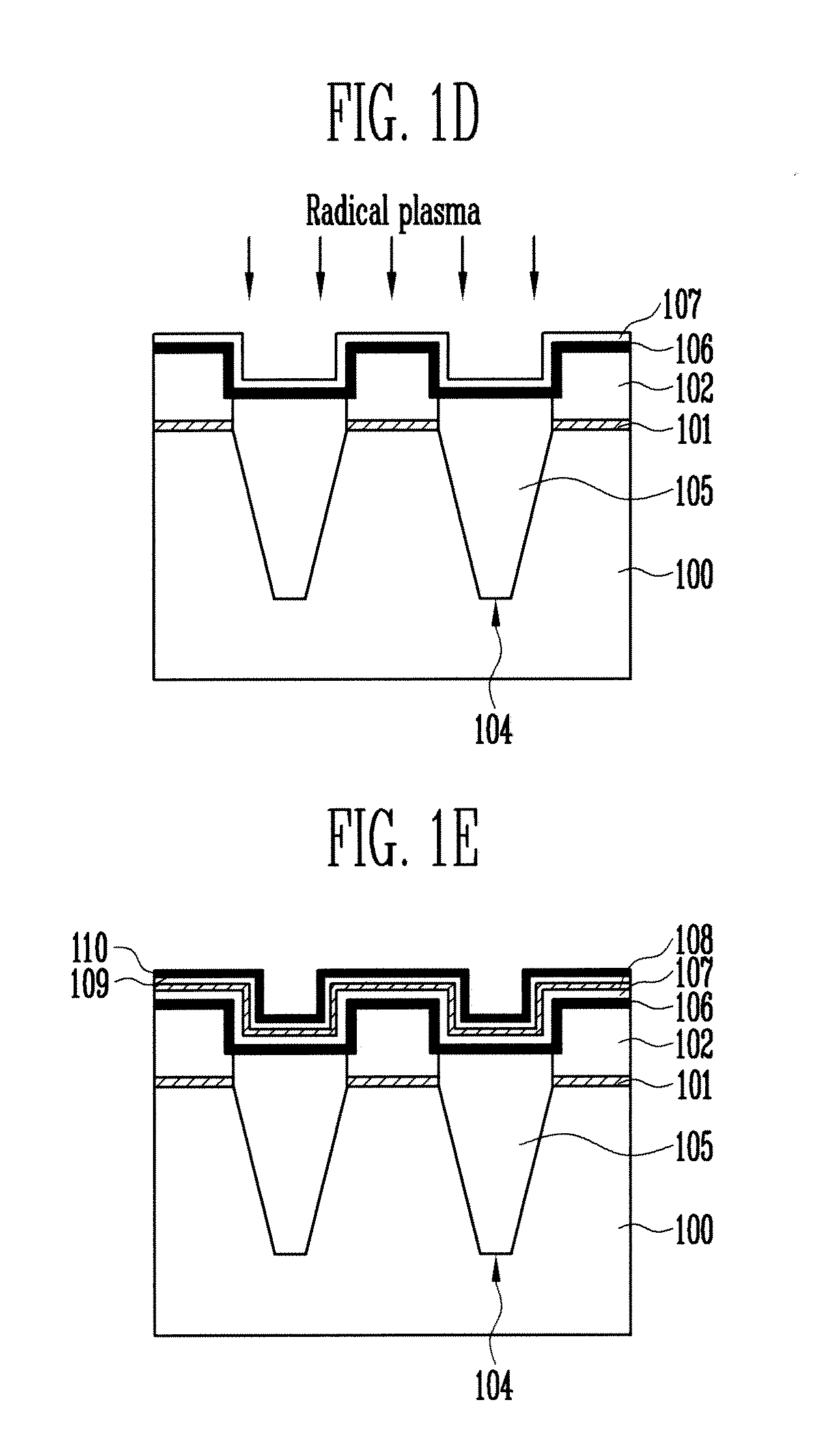
[0037]FIGS. 1A to 1E are cross-sectional views showing a method of manufacturing a nonvolatile memory device according to a

[0038]Referring to FIG. 1A, a tunnel insulating layer 101, a charge trap layer 102, and a hard mask layer 103 are sequentially formed over a semiconductor substrate 100. The tunnel insulating layer 101 preferably is formed of an oxide layer. The charge trap layer 102 preferably is formed of a polysilicon layer, or a nitride layer capable of trapping charges. In the case where the charge trap layer 102 is formed of a polysilicon layer, the charge trap layer 102 preferably comprises a dual layer, having an amorphous polysilicon layer not including impurities and a polysilicon layer including impurities. The hard mask layer 103 preferably has a dual structure of an oxide layer and a nitride layer.

[0039]Referring to FIG. 1B, a first etch process is performed to pattern the hard mask layer 103. A second etch process using the patterned hard mask layer 103 as an etch ...

second embodiment

[0064]FIGS. 6A to 6E are cross-sectional views illustrating a method of manufacturing a nonvolatile memory device according to a

[0065]Referring to FIG. 6A, a tunnel insulating layer 601, a charge trap layer 602, a buffer layer 603, a pad layer 604, and a hard mask layer 605 are sequentially formed over a semiconductor substrate 600. The tunnel insulating layer 601 preferably is formed of an oxide layer. The charge trap layer 602 preferably is formed of a polysilicon layer or a nitride layer capable of trapping charges. In the case where the charge trap layer 602 is formed of a polysilicon layer, the charge trap layer 602 preferably is formed to have a dual layer having an amorphous polysilicon layer not including impurities and a polysilicon layer including impurities. The buffer layer 603 preferably is formed of an oxide layer. The pad layer 604 preferably is formed of a nitride layer. The hard mask layer 605 can be formed to have a dual structure of an oxide layer and a nitride la...

third embodiment

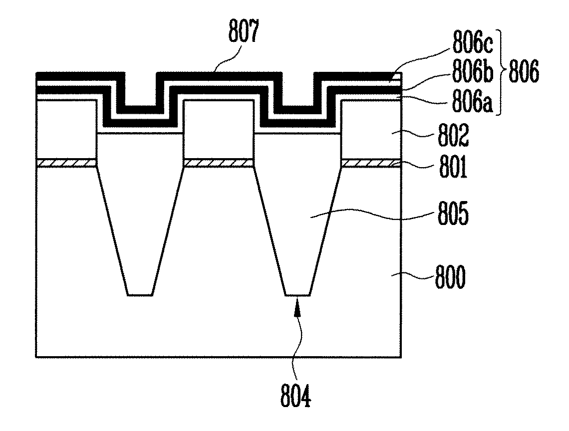
[0080]FIGS. 8A to 8E are cross-sectional views showing a method of manufacturing a nonvolatile memory device according to a

[0081]Referring to FIG. 8A, a tunnel insulating layer 801, a charge trap layer 802, and a hard mask layer 803 are sequentially formed over a semiconductor substrate 800. The tunnel insulating layer 801 preferably is formed of an oxide layer. The charge trap layer 802 preferably is formed of a polysilicon layer or a nitride layer capable of trapping charges. In the case where the charge trap layer 802 is formed of a polysilicon layer, the charge trap layer 802 preferably comprises a dual layer, having an amorphous polysilicon layer not including impurities and a polysilicon layer including impurities. The hard mask layer 803 preferably is formed to have a dual structure of an oxide layer and a nitride layer.

[0082]Referring to FIG. 8B, a first etch process is performed to pattern the hard mask layer 803. A second etch process using the patterned hard mask layer 80...


PUM


Abstract

In one embodiment of a method of manufacturing a nonvolatile memory device, a tunnel insulating layer and a charge trap layer are first formed over a semiconductor substrate that defines active regions and isolation regions. The tunnel insulating layer, the charge trap layer, and the semiconductor substrate formed in the isolation regions are etched to form trenches for isolation in the respective isolation regions. The trenches for isolation are filled with an insulating layer to form isolation layers in the respective trenches. A lower passivation layer is formed over an entire surface including top surfaces of the isolation layers. A first oxide layer is formed over an entire surface including the lower passivation layer. Meta-stable bond structures within the lower passivation layer are removed. A nitride layer, a second oxide layer, and an upper passivation layer are sequentially formed over an entire surface including the first oxide layer.

Description

CROSS-REFERENCE TO RELATED APPLICATION[0001]Priority to Korean patent application number 10-2009-0044514 filed May 21, 2009, the entire disclosure of which is incorporated by reference herein, is claimed.BACKGROUND[0002]One or more embodiments of the disclosure relate to a method of manufacturing a nonvolatile memory device and, more particularly, to a method of manufacturing a nonvolatile memory device, which is capable of improving a retention characteristic by suppressing a charge-sharing phenomenon of a dielectric layer.[0003]In general, nonvolatile memory devices retain data even though the supply of power is stopped. A unit cell of a nonvolatile memory device has a structure in which a tunnel insulating layer, a floating gate, a dielectric layer, and a control gate are sequentially stacked in an active region of a semiconductor substrate. As voltage applied to the control gate from the outside is coupled at the floating gate, the cell can store data. Accordingly, if it is soug...

Claims


Application Information

Patent Timeline
Patent Type & Authority Applications(United States)
IPC IPC(8): H01L21/762
CPCH01L27/11568H01L21/76224H10B43/30H01L21/28202H01L21/31051
Inventor YUN, KWANG HYUN
Owner SK HYNIX INC
Why Eureka
Try Eureka