Si surface cleaning for semiconductor circuits

a technology for semiconductor circuits and surfaces, applied in the field of electronic circuit fabrication, can solve the problems of atomically cleaning si surfaces, compromising performance, and facing ever more challenges

Active Publication Date: 2011-08-09
CISCO TECH INC
View PDF11 Cites 17 Cited by
  • Summary
  • Abstract
  • Description
  • Claims
  • Application Information

AI Technical Summary

Problems solved by technology

As function, and hence complexity, of electronic circuits increases, the art is faced with ever more challenges to stay on the path of delivering better performance.
In many advanced semiconductor circuits, differing components, such as P or N type devices, three dimensional devices, possibly optical devices, may have such variations in their requirements that processing them all in a single material would compromise performance.
A problem encountered in the art is that atomically clean Si surfaces are very difficult to produce, and cleaning a Si surface usually involves high temperature.

Method used


Image

  • Si surface cleaning for semiconductor circuits
  • Si surface cleaning for semiconductor circuits
  • Si surface cleaning for semiconductor circuits

Examples


Embodiment Construction

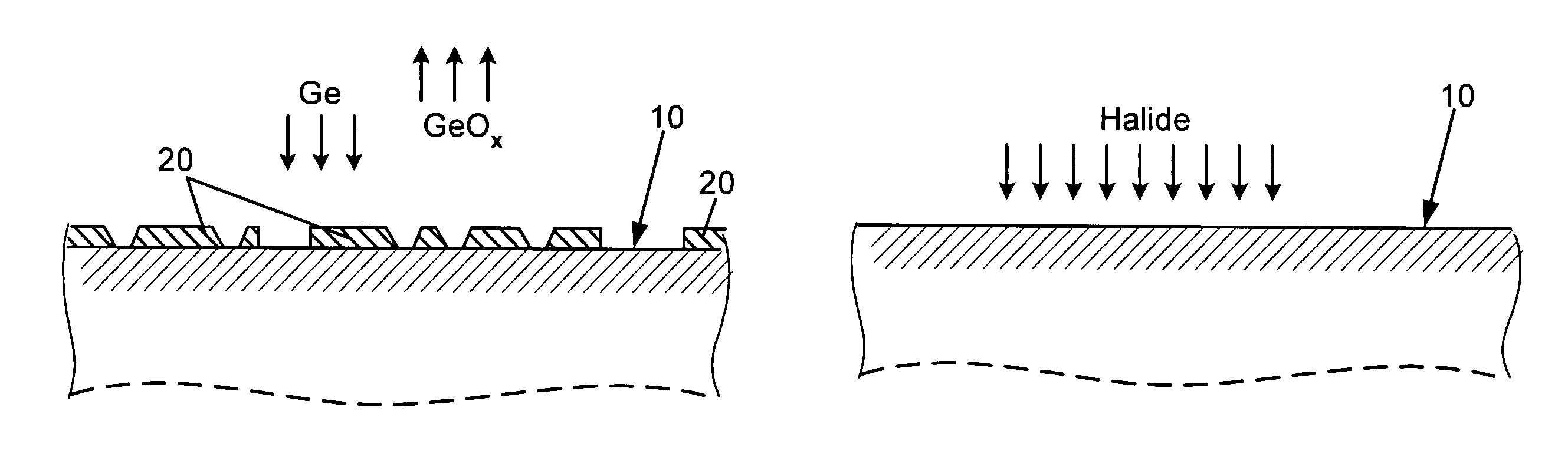
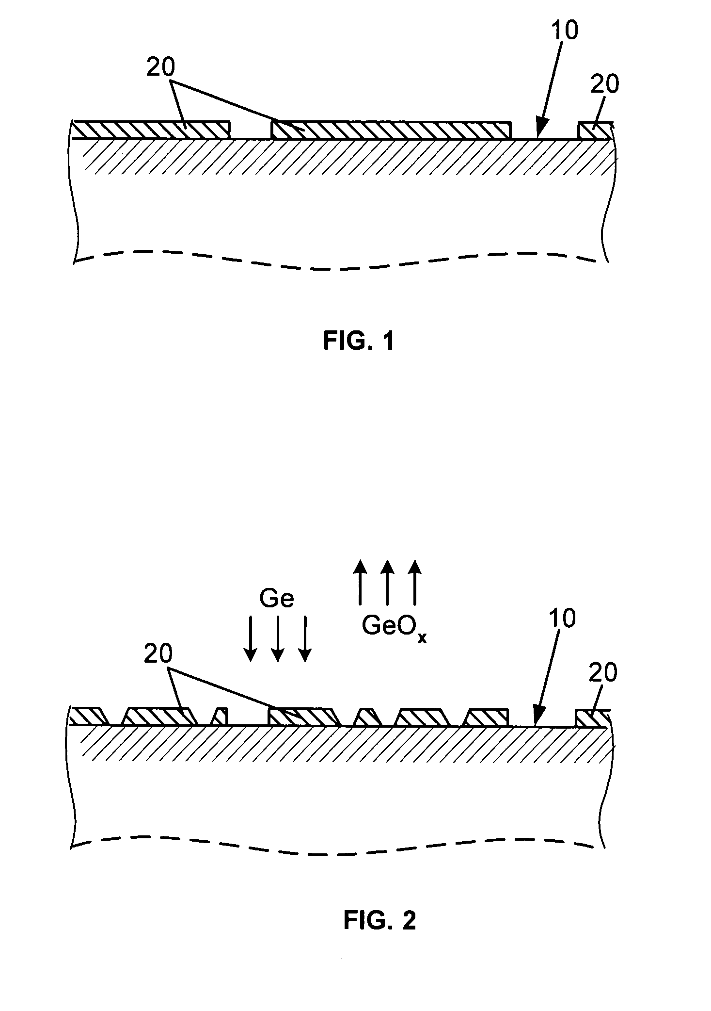
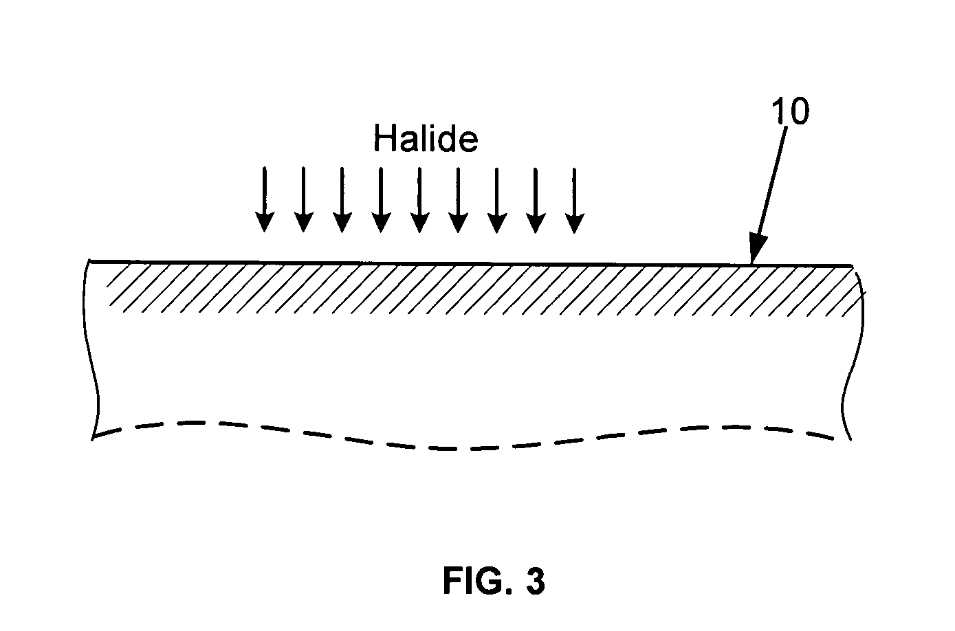
[0012]It well known in the electronics art that depositing epitaxial layers is often necessary during the fabrication of semiconductor circuits. As scaling of circuit components to ever smaller sizes continues, and inclusion of optical devices into circuit chips takes place, the desire for epitaxial deposition at relatively low temperatures increases. The lower the temperature of the epitaxial deposition may be, the more flexibility one has for integrating the fabrication process flow. The reason for this is that a lower temperature process may be less damaging to structures already in place at the time of the epitaxy, or growth. The terms “epitaxial relation”, “epitaxially”, “epitaxy”, “epi”, “epitaxial growth” etc. carry their customary usage: meaning that a layer is formed on a platform, which layer has the same symmetry and crystalline orientation as the platform itself.

[0013]Successful epitaxial deposition requires a clean surface on which the epitaxial growth can take place. I...


PUM


Abstract

A method is disclosed for the cleaning of a Si surface at low temperatures. Oxide on the Si surface is brought into contact with Ge, which then sublimates off the surface. The Ge contamination remaining after the oxide removal is cleared away by an exposure to an alkali halide. The disclosed cleaning method may by used in semiconductor circuit fabrication for preparing surfaces ahead of epitaxial growth.

Description

FIELD OF THE INVENTION[0001]The present invention relates to the fabrication of electronic circuits. In particular, it relates to methods of cleaning a Si surface at low temperatures.BACKGROUND OF THE INVENTION[0002]As function, and hence complexity, of electronic circuits increases, the art is faced with ever more challenges to stay on the path of delivering better performance. The mainstay material of microelectronics is silicon (Si), or more broadly, Si based materials. One such Si based material of importance for microelectronics is the silicon-germanium alloy: Si1-xGex, with “x” indicating the fraction of germanium. In many advanced semiconductor circuits, differing components, such as P or N type devices, three dimensional devices, possibly optical devices, may have such variations in their requirements that processing them all in a single material would compromise performance. Often there is a need to deposit high quality materials, frequently differing kind of materials, dur...

Claims


Application Information

Patent Timeline
Patent Type & Authority Patents(United States)
IPC IPC(8): H01L21/302
CPCH01L21/02046H01L21/02057H01L21/02381H01L21/02661Y10S438/906
Inventor CAPELLINI, GIOVANNIMASINI, GIANLORENZOGUNN, III, LAWRENCE C.WITZENS, JEREMYWHITE, JOSEPH W.
Owner CISCO TECH INC
Why Eureka
Try Eureka