Switch array

a technology of switch array and switch board, which is applied in the direction of contact, microstructural device, coupling device connection, etc., can solve the problems of large relay installation space, large relay can pass and interrupt a minute amount of control current, and cannot be used in some applications such as lighting apparatuses, so as to reduce on-resistance, maintain connection, and increase current flow

Inactive Publication Date: 2011-08-09
TOKYO ELECTRON LTD +1
View PDF14 Cites 3 Cited by
  • Summary
  • Abstract
  • Description
  • Claims
  • Application Information

AI Technical Summary

Benefits of technology

[0008]This simple structure involving the deformation of the deformable member and the maintenance of the deformation enables a large current flow, reduction of the on-resistance, and elimination of the need for a driving current.
[0023]The switch array according to the present invention enables the large current flow, reduction of the on-resistance, and the maintenance of the connection without the driving current.

Problems solved by technology

The relay-embedded board can pass and interrupt a minute amount of control current, but can not be used for some applications such as lighting apparatuses, because switching on and off such lighting apparatuses requires the relays to pass and interrupt a few amperes of current.
One possibility to allow the flow of such a large current is to use a large relay, however, such a large relay requires a relatively large installation space.
Further, if an on-resistance at a relay contact cannot be maintained at 1Ω or lower, the relay causes voltage drop at the relay contact or produces heat at the relay contact when a large current passes through the relay in the on state.
Besides, in order to maintain the on state, a driving current must be kept flowing through a relay's coil which is closed in the on state, therefore increasing a consumption current.
However, such switch arrays have a high on-resistance and cause a large amount of current leakage in the off state, whereby being prone to break the elements during the flow of the large current.

Method used


Image

  • Switch array
  • Switch array
  • Switch array

Examples


Embodiment Construction

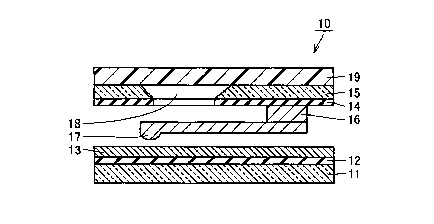
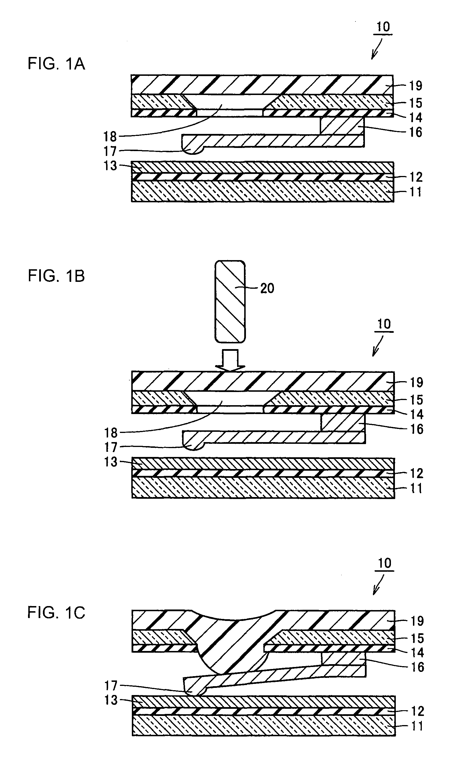
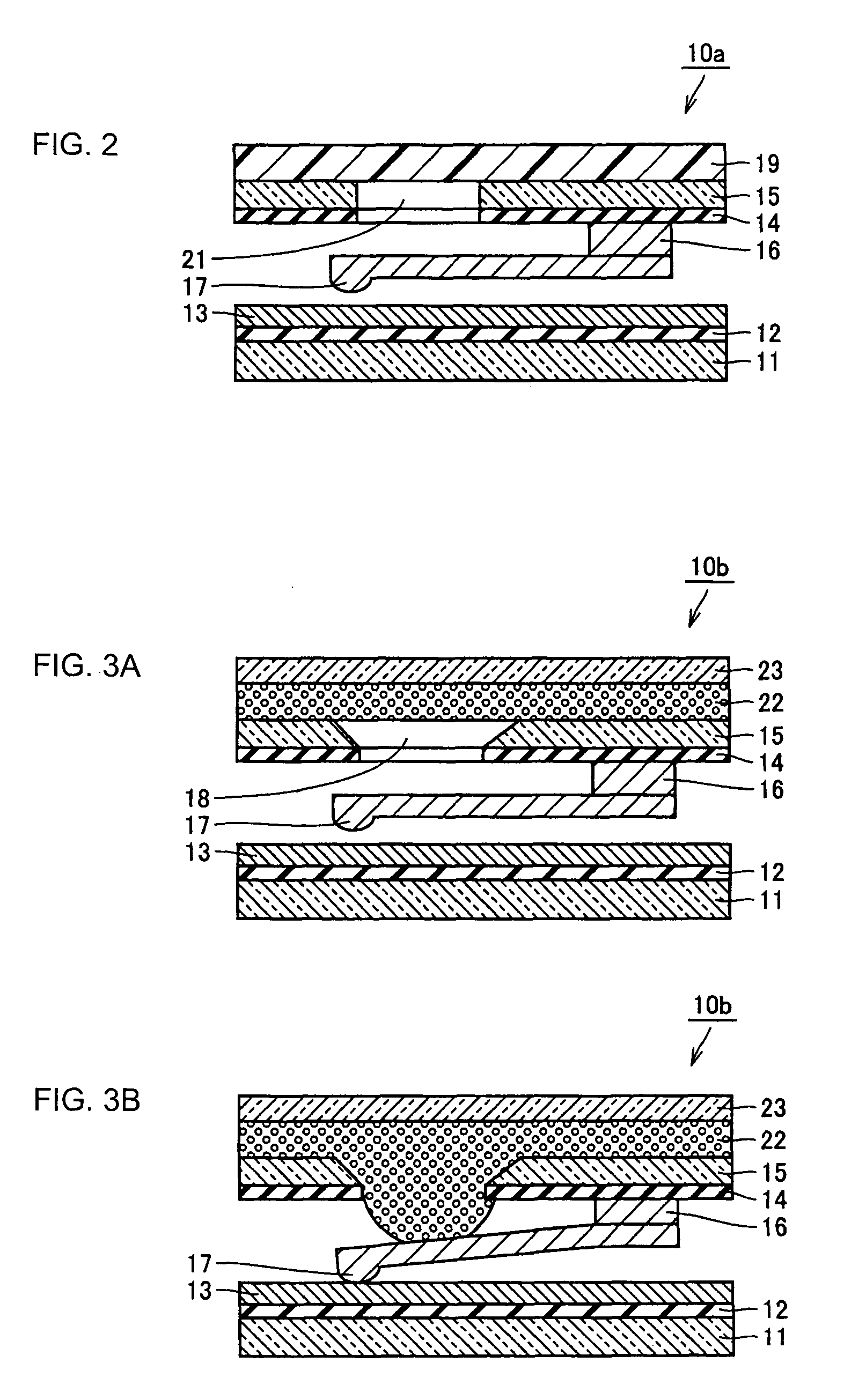
[0051]FIGS. 1A to 1C are cross-sectional views illustrating a switch included in a switch array according to one embodiment of the present invention. In FIG. 1A, a switch 10 is disposed in a cross area of the switch array. An insulating film 14 and an upper substrate 15 are provided in a parallel, spaced apart relationship with respect to a lower substrate 11 and an insulating film 12. A first wiring layer 16 is placed on the lower face of the insulating film 14, while a second wiring layer 13 is placed on the insulating film 12 so as to three-dimensionally cross the first wiring layer 16.

[0052]In the cross area between the first wiring layer 16 and the second wiring layer 13, a cantilever 17 is provided functioning as a deformable member and has one end connected to the first wiring layer 16 and the other end opposed to the second wiring layer 13 with a space therebetween in an insulated state. The cantilever 17 can make a connection with the second wiring layer 13 at the other end...


PUM


Abstract

A first wiring layer 16 is disposed on an insulating film 14 on the lower surface of an upper substrate 15, while a second wiring layer 13three-dimensionally crossing the first wiring layer 16 is provided on the insulating film 12 on a lower substrate 11. A cantilever 17 has one end connected to the first wiring layer 16 and the other end opposed to the second wiring layer 13 with a space therebetween. A thermoplastic sheet 19 is arranged on the upper substrate 15 so as to cover the through-hole 18. The thermoplastic sheet 19 is pressed by a heated pin 20 against the cantilever 17 and deformed so as to maintain the connection between the cantilever 17and the second wiring layer 13, and therefore close the switch 10.

Description

TECHNICAL FIELD[0001]This invention relates to a switch array, and for example, relates to a switch array that makes and breaks any connection of a plurality of input lines and a plurality of output lines.BACKGROUND ART[0002]As an example of a switch array capable of selectively making and breaking any connection of a plurality of input lines and a plurality of output lines, Japanese unexamined patent publication No. 10-283893 discloses a relay-embedded board. This relay-embedded board disclosed in publication No. 10-283893 includes nine ultra small relays embedded on a thin substrate, each relay being placed in each cross area where three inputs and three outputs cross each other. This example allows any desired relays to be switched on and off.[0003]Because the relays of the relay-embedded board disclosed in publication No. 10-283893 are ultra small, the contact capacity of each relay is also small. The relay-embedded board can pass and interrupt a minute amount of control current...

Claims


Application Information

Patent Timeline
Patent Type & Authority Patents(United States)
IPC IPC(8): H01H1/00H01H9/00
CPCB81B3/0054H01H1/0036H01H37/46H01H67/22B81B2201/014B81B2203/053H01H1/24H01H2001/0042H01H2037/008
Inventor HAYASHI, MASATOYAKABE, MASAMIHASEBE, TETSUYAHARADA, MUNEOOKUMURA, KATSUYA
Owner TOKYO ELECTRON LTD
Why Eureka
Try Eureka