Methods for fabricating contacts to pillar structures in integrated circuits

a technology of integrated circuits and pillar structures, applied in the field of integrated circuits, can solve the problems of increasing difficulty, difficult alignment of vias to mtj pillar structures, and limitations of mtj sizes as they become smaller, and achieves the effect of robustness and easy scalabl

Inactive Publication Date: 2011-08-30
GLOBALFOUNDRIES INC
View PDF11 Cites 57 Cited by
  • Summary
  • Abstract
  • Description
  • Claims
  • Application Information

AI Technical Summary

Benefits of technology

[0010]Advantageously, the above-described method embodiment provides a robust and easily scalable process by which to implement various kinds of pillar structures with widths or diameters less than about 100 nm in integrated circuits.

Problems solved by technology

In the process integration of MRAM, for example, one of the challenging processing steps is the formation of a vertical contact between an MTJ pillar structure and an overlying conductive line.
Unfortunately, this problem becomes progressively more difficult as MRAM is scaled to the smaller MTJ dimensions required for the 45 nm and 32 nm ground rule nodes.
Even though this approach works well for relatively large MTJ pillar structures (e.g., those with widths or diameters greater than about 100 nm), it has limitations as MTJ sizes become smaller.
Overlay errors make alignment of the via to the MTJ pillar structure extremely difficult as the size of the MTJ shrinks.
Hence, the via-based approach is not useful for MRAM scaling to 45 nm and 32 nm nodes.
However, patterning the MTJ using a tall conductive hard mask is problematic due to the formation of sidewall redeposition, shown as feature 260 in the figures, that shorts the junctions, and foot structures due to shadowing during etching.
Furthermore, the planarization step usually introduces non-uniformity, which is transferred into the etch process used to form the trench for the conductive line.
Due to these problems, the tall hard mask approach does not provide a straight-forward path for the formation of contacts for MRAM scaling.

Method used


Image

  • Methods for fabricating contacts to pillar structures in integrated circuits
  • Methods for fabricating contacts to pillar structures in integrated circuits
  • Methods for fabricating contacts to pillar structures in integrated circuits

Examples


Embodiment Construction

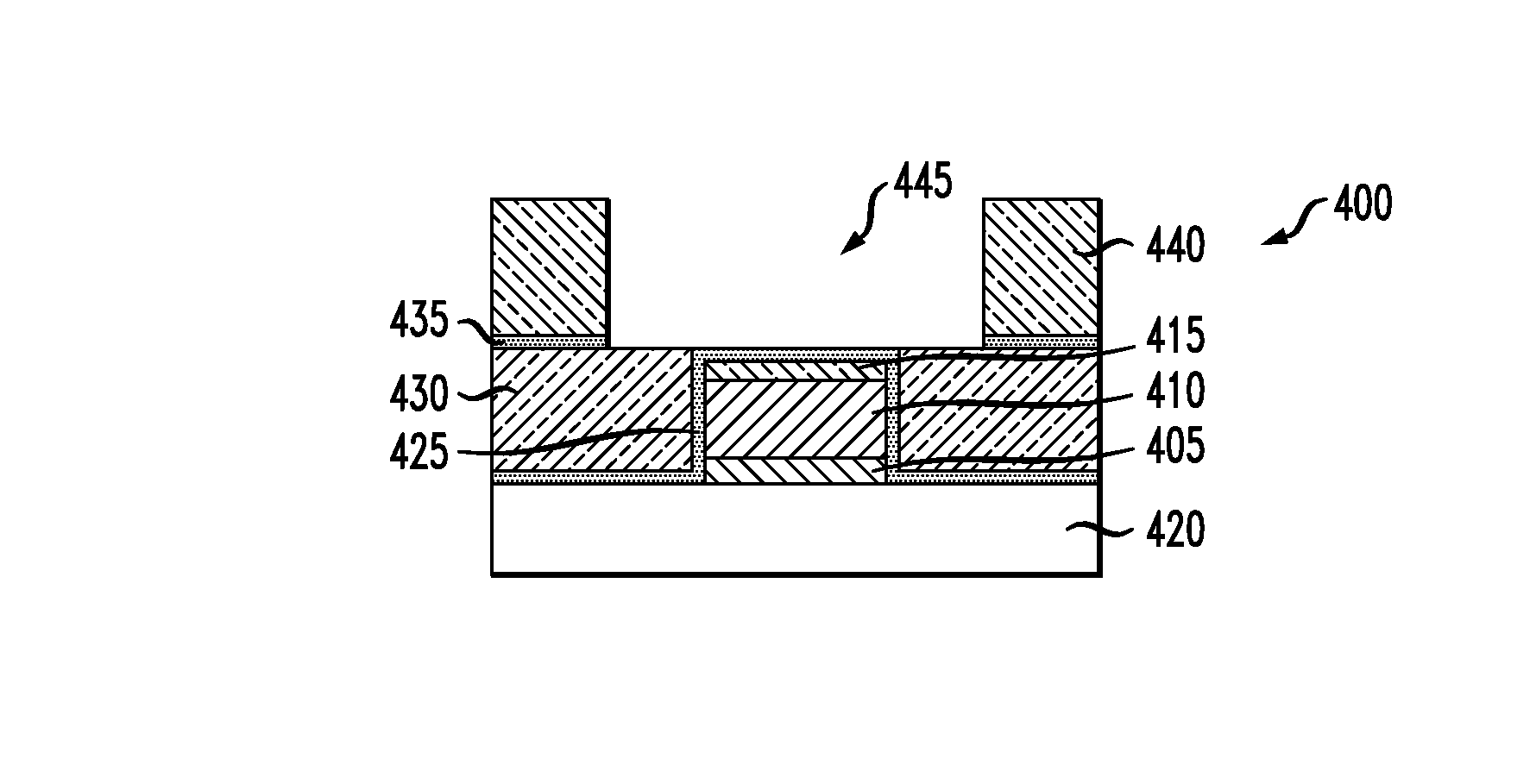
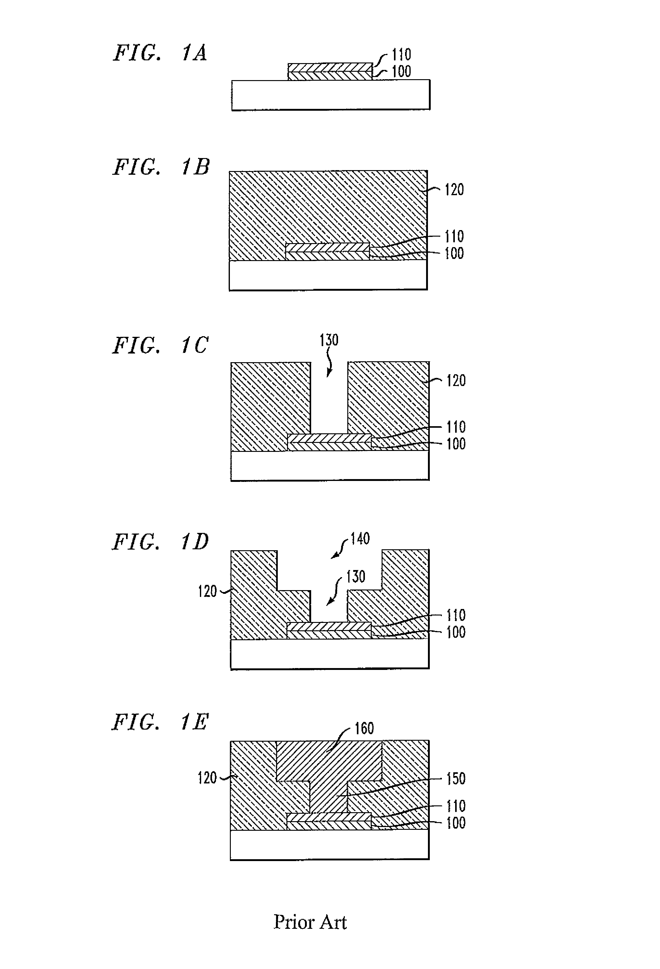
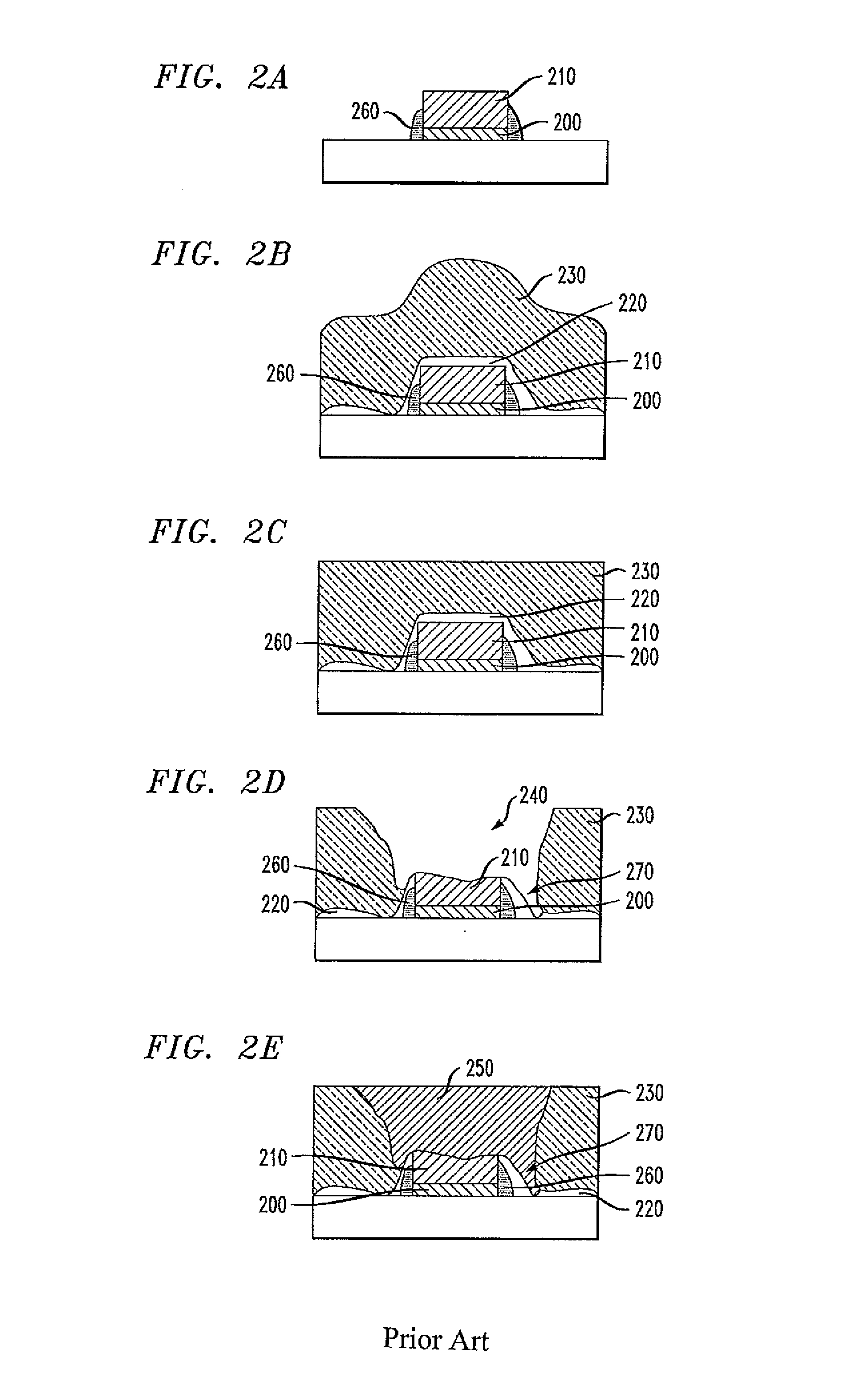
[0017]The present invention will be described with reference to illustrative embodiments. For this reason, numerous modifications can be made to these embodiments and the results will still come within the scope of the invention. No limitations with respect to the specific embodiments described herein are intended or should be inferred.

[0018]Particularly with respect to processing steps, it is emphasized that the descriptions provided herein are not intended to encompass all of the processing steps which may be required to successfully form a functional device. Rather, certain processing steps which are conventionally used in forming integrated circuit devices, such as, for example, wet cleaning and annealing steps, are purposefully not described herein for economy of description. However one skilled in the art will readily recognize those processing steps omitted from this generalized description. Moreover, details of conventional semiconductor processing steps described herein wil...


PUM


Abstract

A pillar structure that is contacted by a vertical contact is formed in an integrated circuit. A hard mask is formed and utilized to pattern a least a portion of the pillar structure. The hard mask comprises carbon. Subsequently, the hard mask is removed. A conductive material is then deposited in a region previously occupied by the hard mask to form the vertical contact. The hard mask may, for example, comprise diamond-like carbon. The pillar structure may have a width or diameter less than about 100 nanometers.

Description

FIELD OF THE INVENTION[0001]This invention relates generally to integrated circuits, and, more particularly, to techniques for forming and contacting pillar structures in integrated circuits.BACKGROUND OF THE INVENTION[0002]Magnetic memory devices, such as magnetic random access memory (MRAM) devices, use magnetic memory cells to store information. Information is stored in a magnetic memory cell as the orientation of the magnetization of a free layer as compared to the orientation of the magnetization of a fixed or pinned layer. The magnetization of the free layer may be oriented parallel or anti-parallel to the fixed layer, representing either a logic “0” or a logic “1.” One type of memory cell, a magnetic tunnel junction (MTJ), consists of a pillar structure comprising a free layer and a fixed layer separated by a thin dielectric barrier (a tunnel barrier), which typically comprises Al2O3, MgO, or MgO sandwiched between thin layers of metal. The resistance of the memory cell depen...

Claims


Application Information

Patent Timeline
Patent Type & Authority Patents(United States)
IPC IPC(8): H01L21/00
CPCH01L43/12H10N50/01
Inventor ASSEFA, SOLOMONCOSTRINI, GREGORYJAHNES, CHRISTOPHER VINCENTROOKS, MICHAEL J.SUN, JONATHAN ZANHONG
Owner GLOBALFOUNDRIES INC
Why Eureka
Try Eureka