Power semiconductor device

a technology of semiconductor devices and semiconductors, applied in the direction of semiconductor devices, basic electric elements, electrical equipment, etc., can solve the problems of large side etching amount of metal films, easy scattering, and difficult shortening so as to reduce the width of edge termination structures, reduce the effect of the width of the edge termination structure, and reduce the scattering of initial forward blocking voltage capability characteristics

Active Publication Date: 2011-08-30
FUJI ELECTRIC CO LTD
View PDF14 Cites 6 Cited by
  • Summary
  • Abstract
  • Description
  • Claims
  • Application Information

AI Technical Summary

Benefits of technology

[0007]In view of the above it would be preferable to provide a power semiconductor device which permits a reduction of the width of the edge termination structure, exhibits superior long-term forward blocking voltage capability reliability, and allows scatter of the forward blocking voltage capability characteristic to be minimized. Preferably, these characteristics would be provided even when the edge termination structure of the power semiconductor device comprises a field plate that employs a metal film for a relatively thick metal electrode, and in cases of a large side etching amount or etching amount scatter when a field plate of a predetermined pattern is processed by wet-etching the metal film that is attached to the whole surface.
[0029]The present invention makes it possible to provide a power semiconductor device which permits a reduction of the width of the edge termination structure, exhibits superior long-term forward blocking voltage capability reliability, and allows scatter of the initial forward blocking voltage capability characteristic to be minimized. These advantages are possible even when the edge termination structure of the power semiconductor device comprises a field plate that employs a metal film for a relatively thick metal electrode, or in cases of a large side etching amount or etching amount scatter when a field plate of a predetermined pattern is processed by wet-etching the metal film that is attached to the whole surface.

Problems solved by technology

However, as mentioned earlier, because the required pattern is processed by wet-etching a metal film that has a relatively large film thickness, with the field plate that is conventionally applied to a power semiconductor element, the amount of side etching of the metal film is large.
Because it is necessary to anticipate each of the widths indicated by the arrows in FIG. 14 in the design by taking the width corresponding with this large amount of side etching as the design margin, it is difficult to shorten the edge termination structure.
In addition, scatter readily occurs in the initial characteristic of the device forward blocking voltage capability because, in comparison with dry etching, wet etching has a low etching accuracy due to the large scatter in the etching amounts and so forth.

Method used


Image

  • Power semiconductor device
  • Power semiconductor device
  • Power semiconductor device

Examples


Embodiment Construction

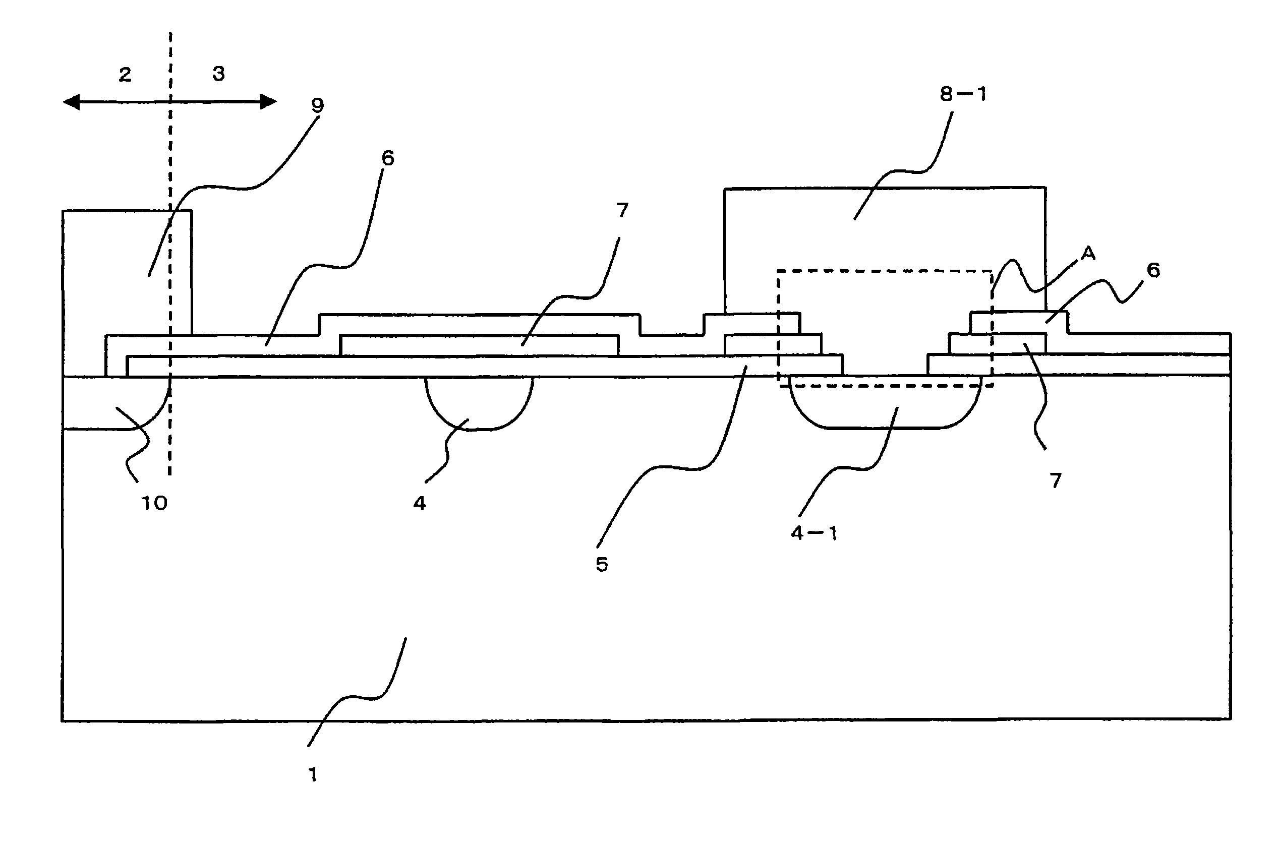
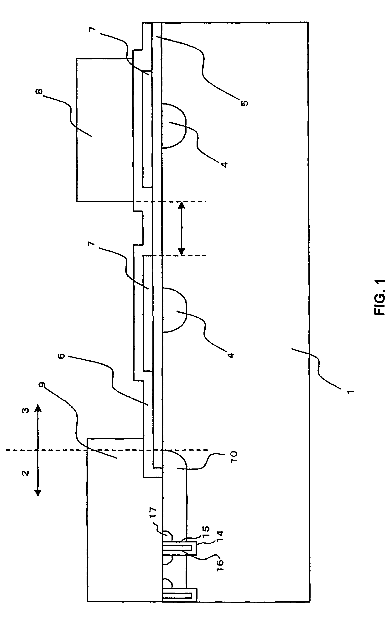
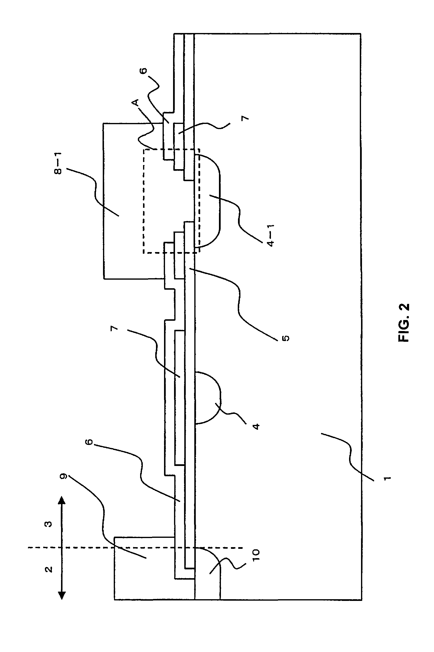
[0050]FIGS. 1 to 4 are planar views of different edge termination structures of the power semiconductor device of the present invention. FIGS. 5 to 7 are cross-sectional views of different edge termination structures in the corner portion of the power semiconductor device of the present invention. FIG. 8 is an enlarged cross-sectional view of the edge termination structure in the corner portion of the power semiconductor device of the present invention. FIGS. 9 to 12 are cross-sectional views along the line X-X′ of the edge termination structure of FIG. 6B which serves to illustrate the method of fabricating the power semiconductor device of the present invention. FIG. 13 is a cross-sectional view along the line Y-Y′ of FIG. 6B which shows a non-contact portion of the edge termination structure in the corner portion of the power semiconductor device of the present invention. FIG. 15 is a (fifth) planar view B of the edge termination structure in the corner portion of the power semic...


PUM


Abstract

A power semiconductor device is provided having a field plate that employs a thick metal film in an edge termination structure and which permits edge termination structure width reduction even with large side etching or etching variation, which exhibits superior long-term forward blocking voltage capability reliability, and which allows minimal forward blocking voltage capability variation. The edge termination structure has multiple ring-like p-type guard rings, a first insulating film covering the guard rings, and ring-like field plates, provided via the first insulating film atop the guard rings. The field plates have a polysilicon film and a thicker metal film. The polysilicon film is provided on a first guard ring via first insulating film, and a dual field plate made of the polysilicon film and metal film is provided on a second guard ring. The dual field plate is stacked via a second insulating film. The first and second guard rings alternate.

Description

BACKGROUND[0001]The present invention relates to a power semiconductor device which is used in a power converter or the like.[0002]An essential part cross-sectional view of an active region 20 in which a main current flows in the center of a conventional power semiconductor device and an edge termination structure section 30 that is located at the circumference that encloses the active region 20 is shown in FIG. 14. The edge termination structure section 30 is a part that is provided to reliably hold this OFF-state voltage between the upper and lower electrodes (the lower electrode is not illustrated) of an n-type semiconductor substrate 100 of the device in an OFF state. As the OFF-state voltage increases, there is a need to increase width of the edge termination structure section 30 (the width of the edge termination structure section 30 in a direction extending from the boundary with the active region 20 toward the outer edge of the semiconductor substrate 100). However, because ...

Claims


Application Information

Patent Timeline
Patent Type & Authority Patents(United States)
IPC IPC(8): H01L29/66
CPCH01L29/0619H01L29/402H01L29/404H01L29/66734H01L29/7811H01L29/7813H01L29/0696
Inventor WAKIMOTO, HIROKIOTSUKI, MASAHITOSHIIGI, TAKASHI
Owner FUJI ELECTRIC CO LTD
Why Eureka
Try Eureka