Photodiode array, method of manufacturing the same, and detecting device

a photodiode array and manufacturing method technology, applied in the direction of solid-state devices, semiconductor devices, radio-controlled devices, etc., can solve the problem of high lattice defect density in the edge portion of the epitaxial multilayer that cannot be derived, and achieve the effect of improving the manufacturing efficiency increasing the reliability of the photodiode array

Active Publication Date: 2011-09-20
SUMITOMO ELECTRIC IND LTD
View PDF1 Cites 4 Cited by
  • Summary
  • Abstract
  • Description
  • Claims
  • Application Information

AI Technical Summary

Benefits of technology

[0007]According to the present invention, in a photodiode array including a Group III-V compound semiconductor, a second conductive-side electrode that is common to photodiodes and that extends to the top surface side of an epitaxial multilayer can be efficiently and reliably formed. It is an object of the present invention to provide such a photodiode array, a method of manufacturing the same, and a detecting device including the photodiode array.

Problems solved by technology

In addition, a high lattice defect density in an edge portion of the epitaxial multilayer is not derived from cleavage or the like.

Method used


Image

  • Photodiode array, method of manufacturing the same, and detecting device
  • Photodiode array, method of manufacturing the same, and detecting device
  • Photodiode array, method of manufacturing the same, and detecting device

Examples


first embodiment

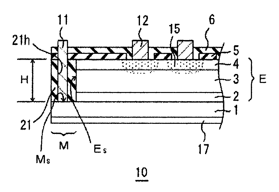
[0041]FIG. 1 is a cross-sectional view of an edge portion of a photodiode array 10 according to a first embodiment of the present invention. An epitaxial multilayer E including an InP buffer layer 2, an absorption layer 3, and an InP window layer 4 is disposed on an n+-type InP substrate 1 doped with sulfur (S). The absorption layer 3 may be composed of any Group III-V compound semiconductor. For example, In0.53Ga0.47As may be used as the absorption layer 3. In the case of In0.53Ga0.47As, the photodiode array 10 has responsivity at a wavelength of 1.7 μm or less in the near infrared. Each photodiode includes a p-type region 15 formed by selectively diffusing zinc (Zn) through an opening of a mask pattern 5 for selective diffusion. In each photodiode, a p-n junction or a p-i-n junction is formed at an end of the p-type region 15.

[0042]A p-side electrode 12, which is a first conductive-side electrode, is provided for each photodiode in order to read photogenerated charges generated by...

second embodiment

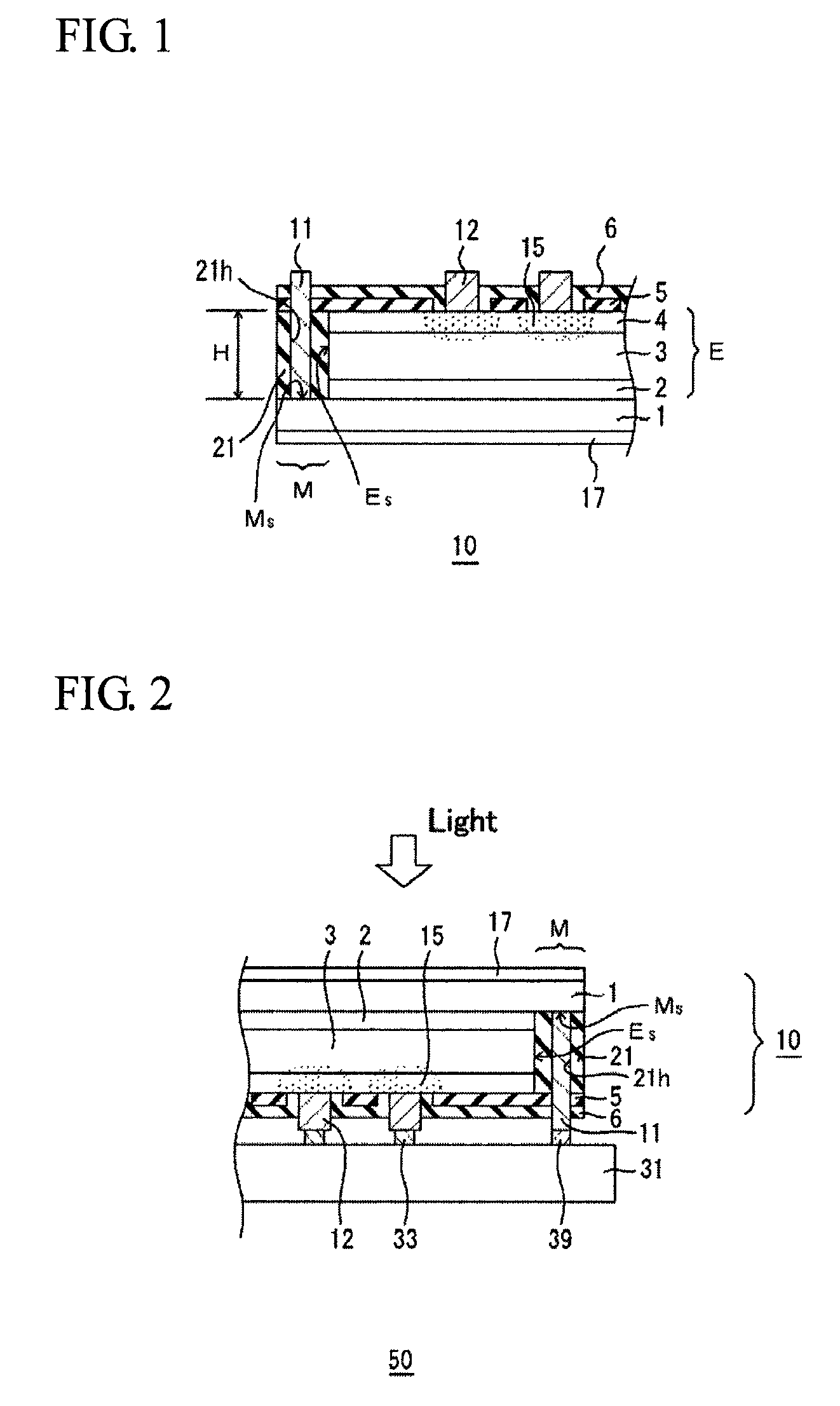
[0060]FIG. 7 is a view showing a photodiode array 10 according to a second embodiment of the present invention. Referring to FIG. 7, an insulating film 21e is disposed between a common n-side electrode 11 and an epitaxial multilayer E. Also in this embodiment, a non-growth part M where the common n-side electrode 11 is to be formed is ensured by a selective growth mask 21. That is, etching of an edge portion of the epitaxial multilayer E for the purpose of formation of the n-side electrode 11 is not performed. Accordingly, in FIG. 7, a surface Ms of the non-growth part M of an InP substrate 1 is a non-processed flat surface continuous from the inside of the InP substrate 1. In addition, a wall surface Es of the edge of the epitaxial multilayer E is a smooth, flat surface. Except for the structures of the n-side electrode 11, the insulating film 21e etc. disposed near the non-growth part M, other structures are the same as those of the photodiode array 10 shown in FIG. 1.

[0061]In man...

third embodiment

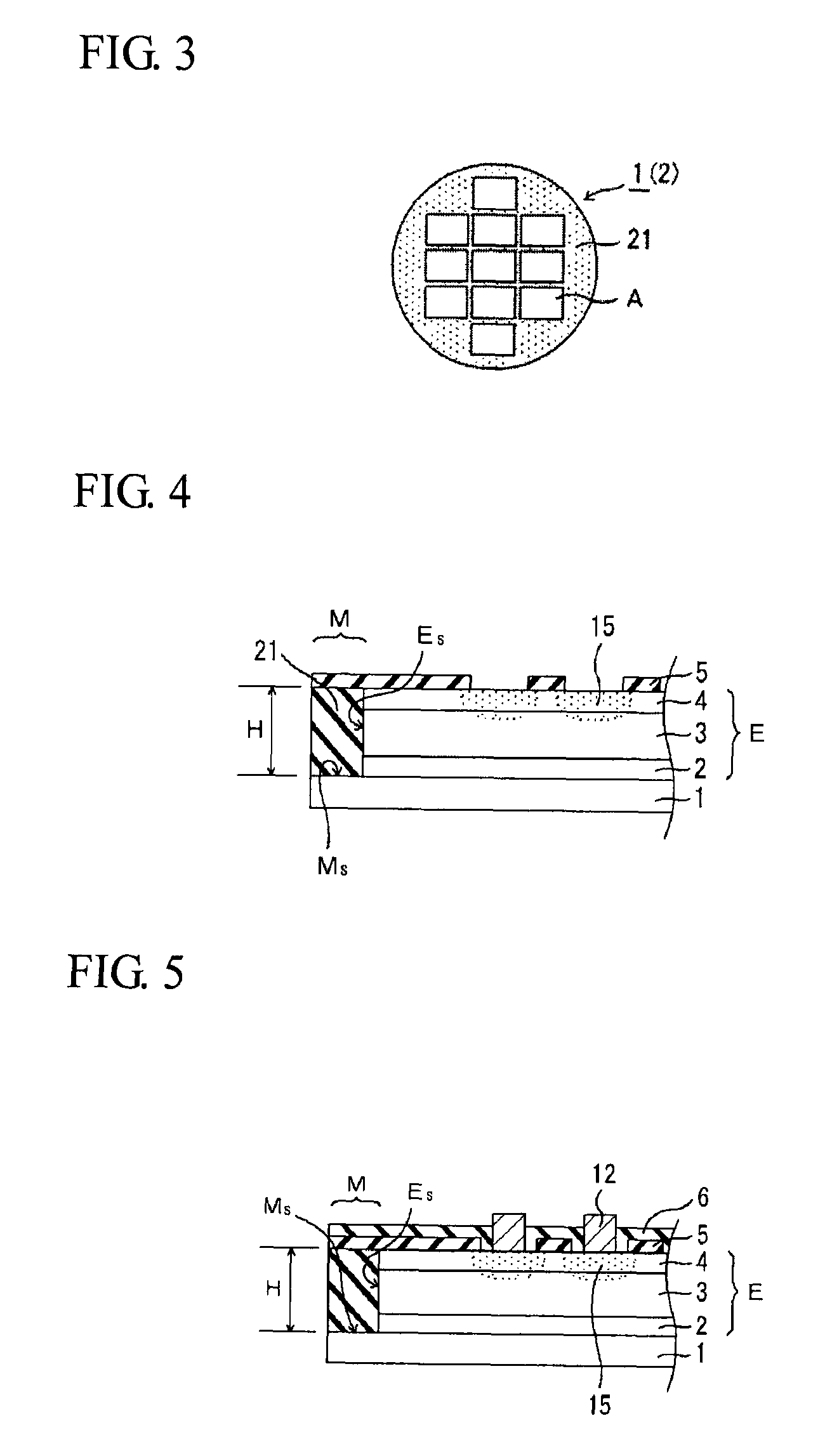
[0067]FIG. 8 is a view showing a photodiode array 10 according to a third embodiment of the present invention. Referring to FIG. 8, a protective film 6 and a selective diffusion mask 5 are disposed between an n-side electrode 11 and an epitaxial multilayer E. Also in this embodiment, a non-growth part M where the common n-side electrode 11 is to be formed is ensured by a selective growth mask 21. That is, etching of an edge portion of the epitaxial multilayer E for the purpose of formation of the n-side electrode 11 is not performed. Accordingly, in FIG. 8, a surface Ms of the non-growth part M of an InP substrate 1 is a non-processed flat surface continuous from the inside of the InP substrate 1. In addition, a wall surface Es of the edge of the epitaxial multilayer E is a smooth, flat surface. Except for the structures of part of the n-side electrode 11, the protective film 6, and the selective diffusion mask 5, the part being located near the non-growth part M, other structures a...


PUM

PropertyMeasurementUnit
diameteraaaaaaaaaa
thicknessaaaaaaaaaa
thicknessaaaaaaaaaa

Abstract

A photodiode array includes a p-side electrode provided on each p-type region formed by selective diffusion and an n-side electrode connected to a non-growth part of an InP substrate and extends to the top surface side of an epitaxial multilayer. A wall surface of an edge at the non-growth part side of the epitaxial multilayer is a smooth surface. A lattice defect density in a portion of the edge of the epitaxial multilayer is higher than a lattice defect density in the inside of the epitaxial multilayer. Furthermore, the non-growth part of the InP substrate to which the n-side electrode is connected has a flat surface continuous from the inside of the InP substrate.

Description

BACKGROUND OF THE INVENTION[0001]1. Field of the Invention[0002]The present invention relates to a photodiode array, a method of manufacturing the same, and a detecting device. More specifically, the present invention relates to a photodiode array having responsivity in the near infrared, a method of manufacturing the same, and a detecting device, such as an image pickup device or a sensor, including the photodiode array.[0003]2. Description of the Related Art[0004]A photodiode array including an absorption layer composed of InGaAs having responsivity in the near infrared is used in imaging using space light, a sensor for a biologically relevant substance etc. Accordingly, many research and development have been carried out. In such a photodiode array including an absorption layer composed of InGaAs, an electrode (p-side electrode) of each photodiode (pixel) has the following structure. The p-side electrode of each photodiode is connected to a p-type region where Zn (p-type impurity...

Claims


Application Information

Patent Timeline
Patent Type & Authority Patents(United States)
IPC IPC(8): H01L31/068H01L27/144H01L27/146H01L31/10
CPCB82Y20/00H01L27/14649H01L27/14694H01L31/035236Y02E10/547
Inventor NAGAI, YOUICHI
Owner SUMITOMO ELECTRIC IND LTD
Why Eureka
Try Eureka