

Semiconductor device
a technology of semiconductor devices and shielding transistors, applied in semiconductor devices, semiconductor/solid-state device details, electrical apparatus, etc., can solve the problems of esd tolerance degradation, device sensitive to damage caused, electrostatic discharge, etc., and achieve the effect of improving the esd tolerance of an esd protection transistor
- Summary
- Abstract
- Description
- Claims
- Application Information
AI Technical Summary
Benefits of technology
Problems solved by technology
Method used
Image

Examples
first embodiment
(Sixth Modification of First Embodiment)
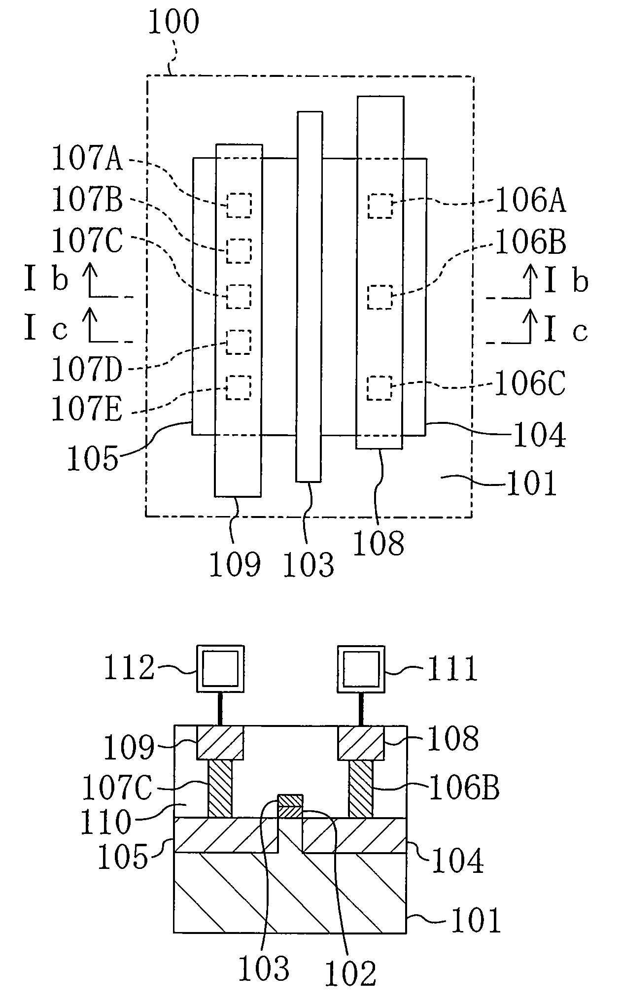
[0092]FIG. 9 shows a plan structure of an ESD protection transistor according to a sixth modification of the first embodiment of the present invention.
[0093]Referring to FIG. 9, in the ESD protection transistor 100 according to the sixth modification, two gate electrodes 103A and 103B are formed between and in parallel with the drain region 104 and the source region 105 to establish two-stage series connection of the transistors. That is to say, the transistor 100 in this modification is a so-called cascade transistor.
[0094]In this structure, the adjacent intervals between the drain contacts 106A to 106C in the gate width direction are set at a value ranging from 1.1 to 5 times the design rule minimum, and the adjacent intervals between the source contacts 107A to 107E in the gate width direction are set at the design rule minimum.
[0095]This provides an increased resistance between the adjacent ones of the drain contacts 106A to 106C, so that,...
second embodiment
(Third Modification of Second Embodiment)
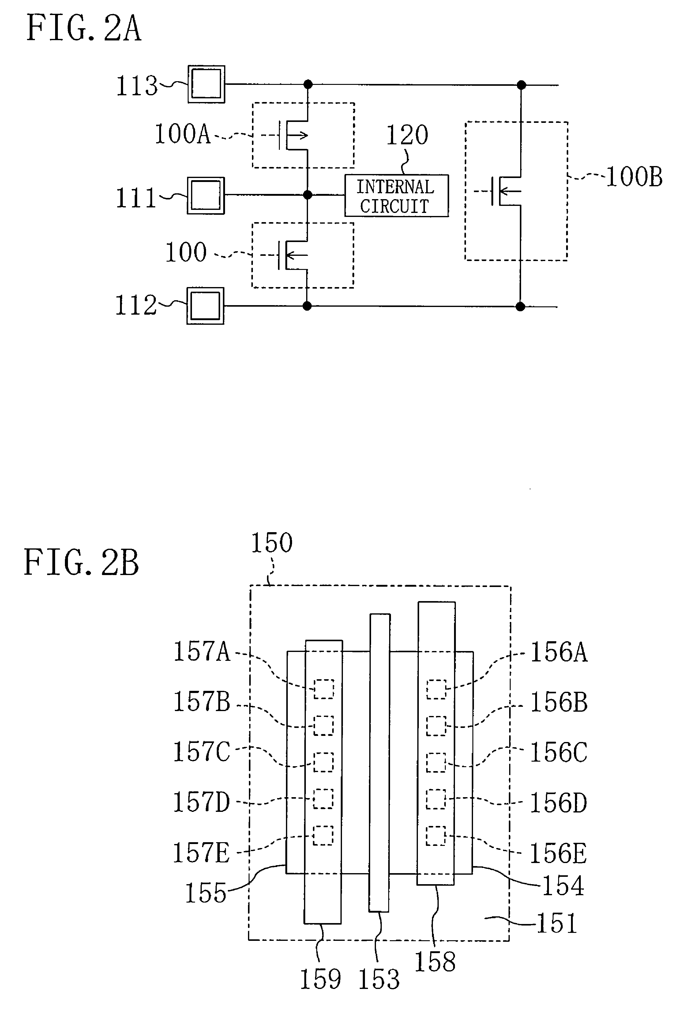
[0123]FIG. 14 shows a plan structure of an ESD protection transistor according to a third modification of the second embodiment of the present invention.
[0124]Referring to FIG. 14, in the ESD protection transistor 200 according to the third modification, a plurality of collector contacts 206A to 206C and a plurality of emitter contacts 207A to 207C are aligned, respectively, in two lines in parallel with the transistor width direction. Furthermore, the adjacent intervals between the collector contacts 206A to 206C and between the emitter contacts 207A to 207C in the transistor width direction are both set at a value ranging from 1.1 to 5 times the design rule minimum. To be more specific, as compared with the structure of the first modification of the second embodiment shown in FIG. 12, the structure of the third modification is constructed so that the collector contacts 206A to 206C and the emitter contacts 207A to 207C are arranged, respect...
PUM
 Abstract
Description
Claims
Application Information