Semiconductor device having seal ring structure

a technology of sealing ring and semiconductor, which is applied in the direction of semiconductor devices, semiconductor/solid-state device details, electrical equipment, etc., can solve the problems of low mechanical strength, poor adhesion of low-k film, and inability to prevent film detachment and cracks during wafer dicing process, so as to improve moisture resistance, prevent film detachment and cracks, and enhance the adhesion between metal layers

Inactive Publication Date: 2011-10-18
RENESAS ELECTRONICS CORP
View PDF7 Cites 0 Cited by
  • Summary
  • Abstract
  • Description
  • Claims
  • Application Information

AI Technical Summary

Benefits of technology

[0017]According to the exemplary configuration of the present invention, while the second metal layer is formed so as to be in contact with the first metal layer, the metal material constituting the second metal layer bulge into the through hole in the first metal layer. To be more specific, the seal ring is entirely made of the metal material except for the insulating material formed on a lower part of the through hole. Accordingly, a larger contact area between the metal layers is obtained, and the adherence between the metal layers can be enhanced. Therefore, it is possible to prevent film detachment and cracks that occur during a dicing process from spreading into the element-forming region located in the chip interior. It is also possible to improve moisture resistance. Hence, the yield of the semiconductor device can be improved.
[0018]Furthermore, while the metal material constituting the second metal layer bulge into the through hole in the first metal layer, the insulating material is formed on a lower part of the through hole. To be more specific, it is configured that a downwardly-projecting convex part formed on the bottom surface of the second metal layer is buried into the through hole formed in the first metal layer. Accordingly, the bottom surface of the second metal layer in the through hole is located at a height different from that of the bottom surface of the second metal layer in the other region and that of the bottom surface of the through hole in the first metal layer. As a result, there is a variation in the level of the interface between metal layers. According to such a configuration, even if horizontal stress caused by impact during a dicing process spreads to the seal ring, resulting in generating a crack, for example, between the first metal layer and the second metal layer, the crack having spread into a certain through hole in the first metal layer is stopped, in the inside of the through hole, at a wall surface of the first metal layer, so that the further progress of the crack can be prevented. Hence, it is possible to improve the yield of the semiconductor device.
[0019]Furthermore, the seal ring according to the present invention can be produced, without adding any new step, simply by preparing a wiring and a via forming a multi-layer wiring structure in a single damascene process or a dual damascene process while forming, in the seal ring part, a pattern different from a pattern of the element-forming region. In addition, when the groove for forming the seal ring is formed in the seal ring part, an insulating film is left in the groove; thus, it is possible to prevent dishing in the process of removing the metal material by using CMP.
[0020]According to the present invention, it is possible to improve the yield of a semiconductor device by preventing film detachment and cracks that occur during a dicing process from spreading into the chip interior.

Problems solved by technology

Being available in a great variety of types, a “low-k film” generally has poor adherence and low mechanical strength.
Accordingly, there has been a problem that the spread of film detachment and cracks that occur during a wafer dicing process cannot be prevented.
However, in such a configuration, if a crack or film detachment 40 occurs from the dicing line side located in the right side of the drawing, there has been a problem in which such a crack or film detachment 40 propagates to the inside through a part between the via and the wiring, and then develops into a crack or film detachment in the chip interior.
Hence, no solution is provided to the problem in which detachment and cracks from the outer circumference are to spread into the interior.
Accordingly, in the case where film detachment occurs, there is still a problem of detachment and cracks spreading from the outer circumference to the junction of the seal ring and then also into the interior.

Method used


Image

  • Semiconductor device having seal ring structure
  • Semiconductor device having seal ring structure
  • Semiconductor device having seal ring structure

Examples


Embodiment Construction

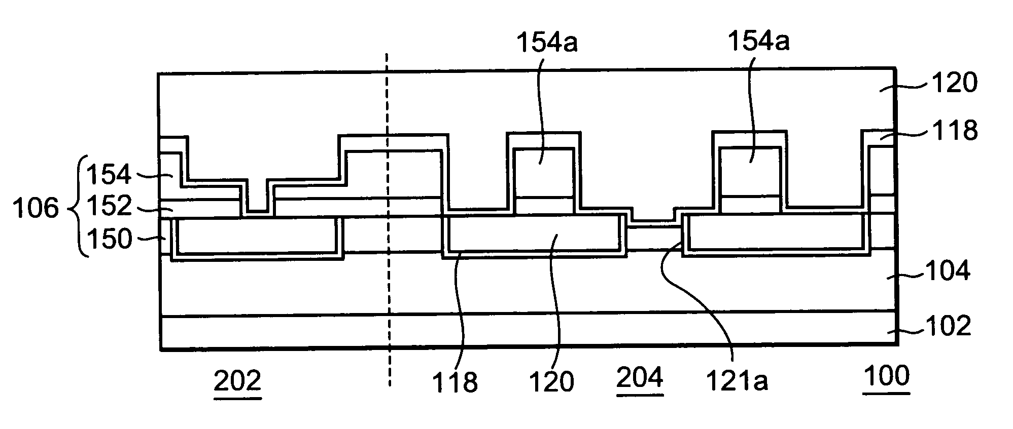
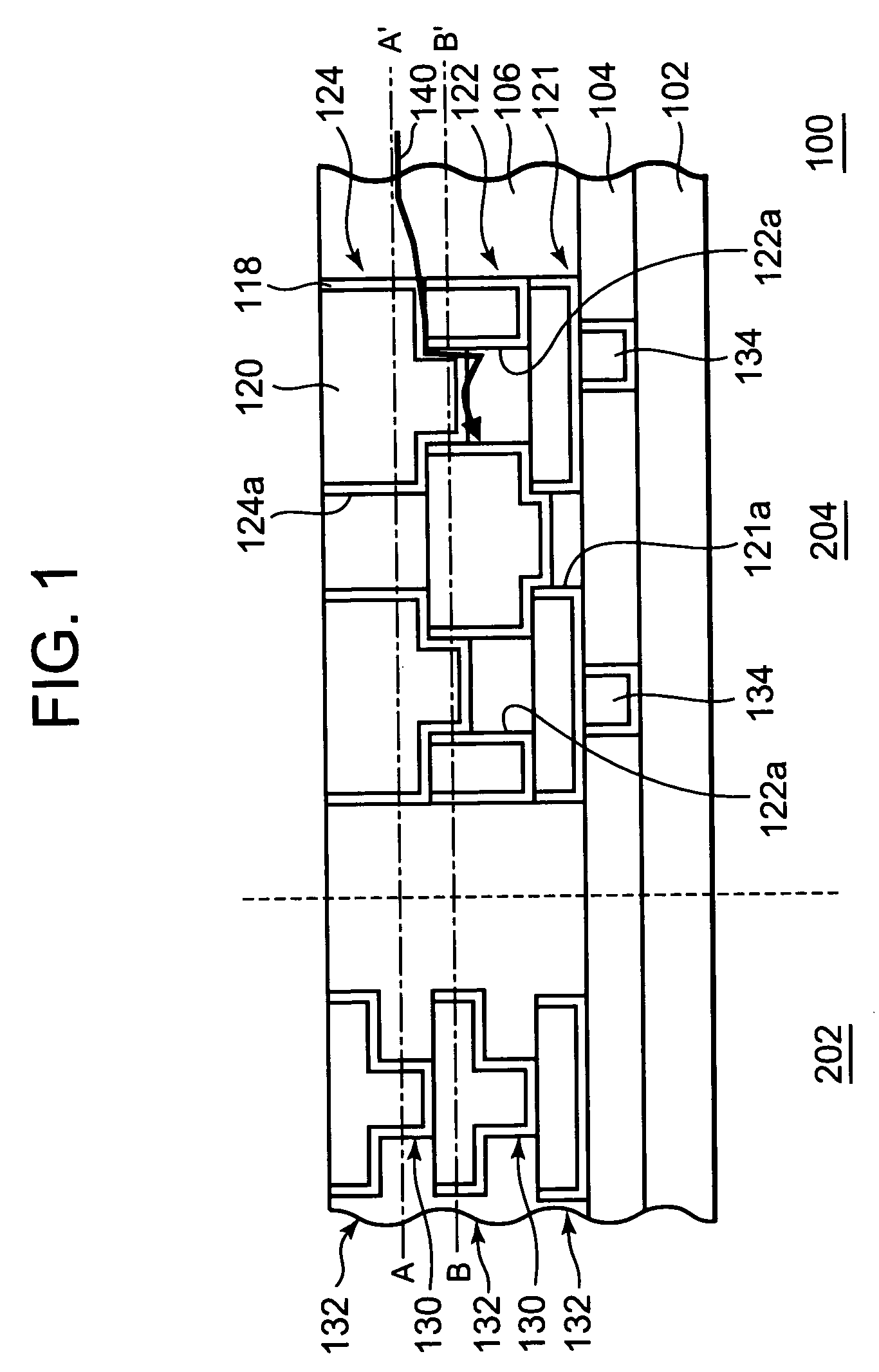
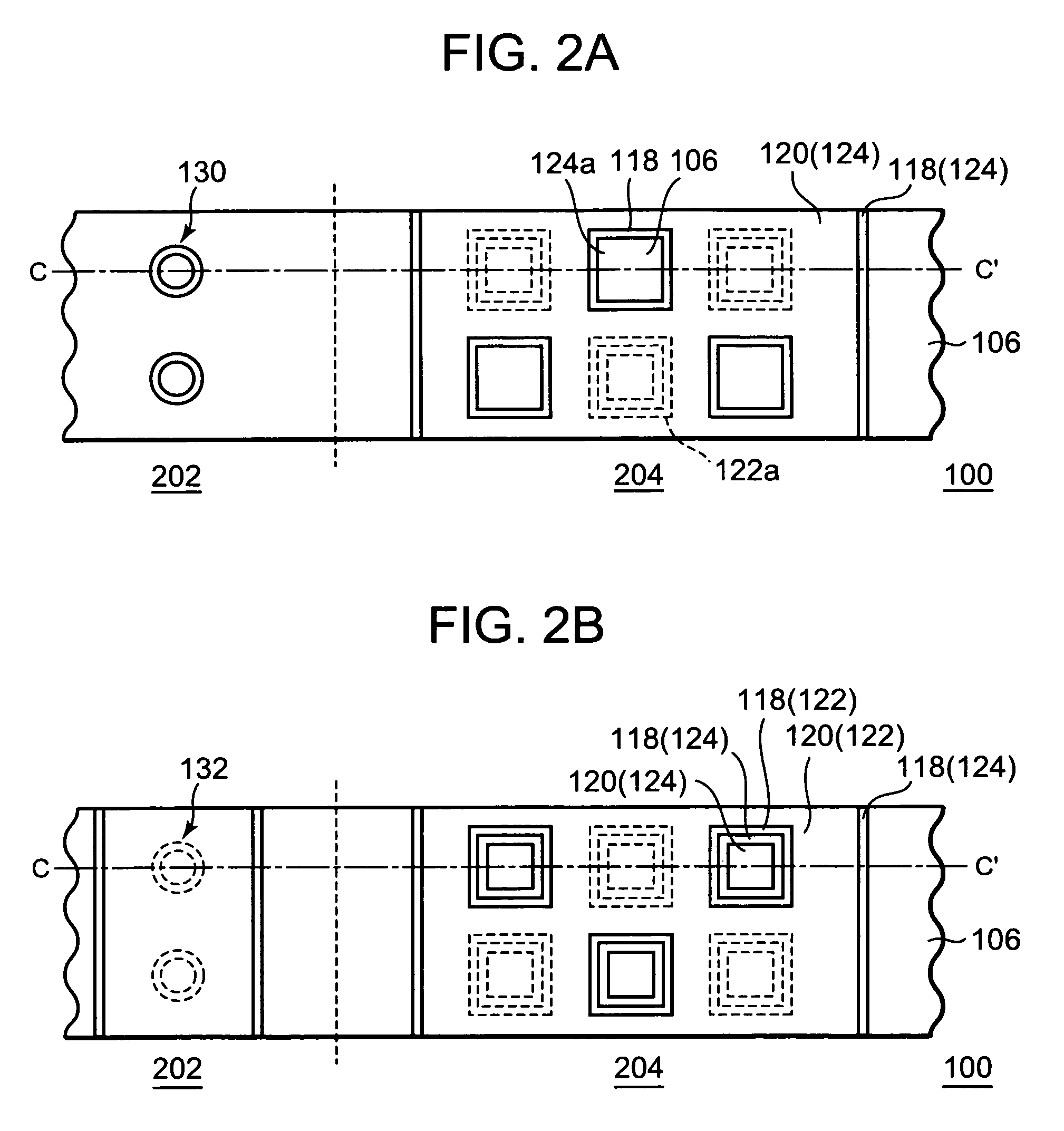
[0048]FIG. 1 is a cross-sectional view illustrating a configuration of a semiconductor device according to an exemplary embodiment of the present invention. FIG. 2 is a lateral plan view of the semiconductor device 100 illustrated in FIG. 1. FIG. 2A corresponds to a cross-sectional view taken along the line A-A′ of FIG. 1, while FIG. 2B corresponds to a cross-sectional view taken along the line B-B′ of FIG. 1. FIG. 1 corresponds to a cross-sectional view taken along the line C-C′ of each of FIG. 2A and FIG. 2B.

[0049]The semiconductor device 100 includes: a substrate 102, which is, for example, a silicon substrate provided with a element (not shown in the drawing), such as a transistor, formed thereon; a lower layer insulating film 104 formed on the substrate 102; and an interlayer insulating film 106 being formed on the lower-layer insulating film 104 and including a low dielectric constant film. The lower-layer insulating film 104 can be composed of a SiO2 film, for example. In the...


PUM

PropertyMeasurementUnit
dielectric constantaaaaaaaaaa
temperatureaaaaaaaaaa

Abstract

A semiconductor device of the present invention includes a seal ring structure. The seal ring structure includes a first metal layer including a though hole, the through hole having a bottom portion filled with an insulating material, and a second metal layer formed on the first metal layer. The second metal layer has a projected portion projecting from a bottom of the second metal layer and the projected portion is inserted into a top portion of the through hole.

Description

BACKGROUND OF THE INVENTION[0001]1. Field of the Invention[0002]The present invention relates to a semiconductor device and a method of producing the same.[0003]2. Description of Related Art[0004]In recent years, in accordance with the progress in the performance of semiconductor devices, a technique for forming an insulating film, so-called “low-k film (low dielectric constant insulating film)” having a lower relative dielectric constant than SiO2 has come to be used in a semiconductor device production process. Being available in a great variety of types, a “low-k film” generally has poor adherence and low mechanical strength. Accordingly, there has been a problem that the spread of film detachment and cracks that occur during a wafer dicing process cannot be prevented.[0005]FIGS. 26A and 26B are drawings illustrating a seal ring structure of a related art. A seal ring, which is a bulkhead provided along the periphery of a semiconductor chip in order to prevent moisture from getti...

Claims


Application Information

Patent Timeline
Patent Type & Authority Patents(United States)
IPC IPC(8): H01L23/40
CPCH01L21/76811H01L23/585H01L21/76808H01L2924/0002H01L2924/00
Inventor USAMI, TATSUYA
Owner RENESAS ELECTRONICS CORP
Why Eureka
Try Eureka