Solid-state imaging device and method for producing the same

a solid-state imaging and imager technology, applied in the direction of semiconductor devices, radio frequency controlled devices, electrical devices, etc., can solve the problems of large problem of resist pattern peeling at the time, shielding film b>10/b>i>e /i>, etc., to reduce the size of pixels, small pattern size, good yield

Active Publication Date: 2008-09-04
PANASONIC SEMICON SOLUTIONS CO LTD
View PDF5 Cites 0 Cited by
  • Summary
  • Abstract
  • Description
  • Claims
  • Application Information

AI Technical Summary

Benefits of technology

[0014]The object of the present invention is to provide a solid-state imaging having a good yield in which a light-shielding film having a small pattern size can be formed so that the size of the pixels can be reduced, and a method for producing the same. In other to achieve this object, the present invention has the following features.
[0015]A first aspect of the present invention is directed to a solid-state imaging device outputting an electrical signal in accordance with an amount of incident light, comprising a light-receiving portion that is formed on a semiconductor substrate; and a light-shielding film in which an opening portion is formed above the light-receiving portion. The light-shielding film includes at least one of a high melting point metal film and a high melting point metal compound film having a light-shielding property. The greatest feature of this invention is that a surface of the light-shielding film has a property of adsorbing or bonding to a hydroxyl group when it is in contact with air. By using the light-shielding film having such characteristics, the adherence between the light-shielding film and the resist is increased, and even if the pattern size is small, the resist pattern can be prevented from being peeled after exposure and development. Consequently, the size of the pixels can be reduced.
[0019]With such a production method, a solid-state imaging device with small pixels can be produced with a good yield.
[0020]Thus, according to the present invention, the surface of the light-shielding film is constituted by either one of a high melting point metal film containing silicon, an amorphous silicon film, a high melting point metal silicide film and an oxide film, and the surface of the film is provided with a property of adsorbing or bonding to a hydroxyl group when it is in contact with air. Therefore, when the light-shielding film is exposed to light and developed for pattern formation, the film can be easily bonded to a surfactant, so that the adherence between the light-shielding film and the resist can be increased. As a result, a solid-state imaging device with a good yield in which even if the pattern size of the light-shielding film is small, the resist pattern can be prevented from being peeled, and the size of the pixels can be reduced, and a method for producing the same can be realized.

Problems solved by technology

With this, peeling of the resist pattern 7 at the time of patterning the light-shielding film 10e has become a large problem.

Method used


Image

  • Solid-state imaging device and method for producing the same
  • Solid-state imaging device and method for producing the same
  • Solid-state imaging device and method for producing the same

Examples


first embodiment

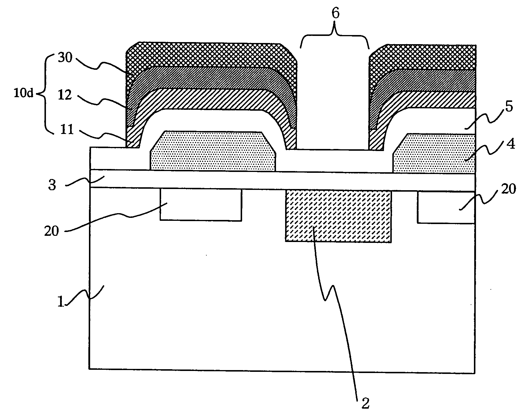
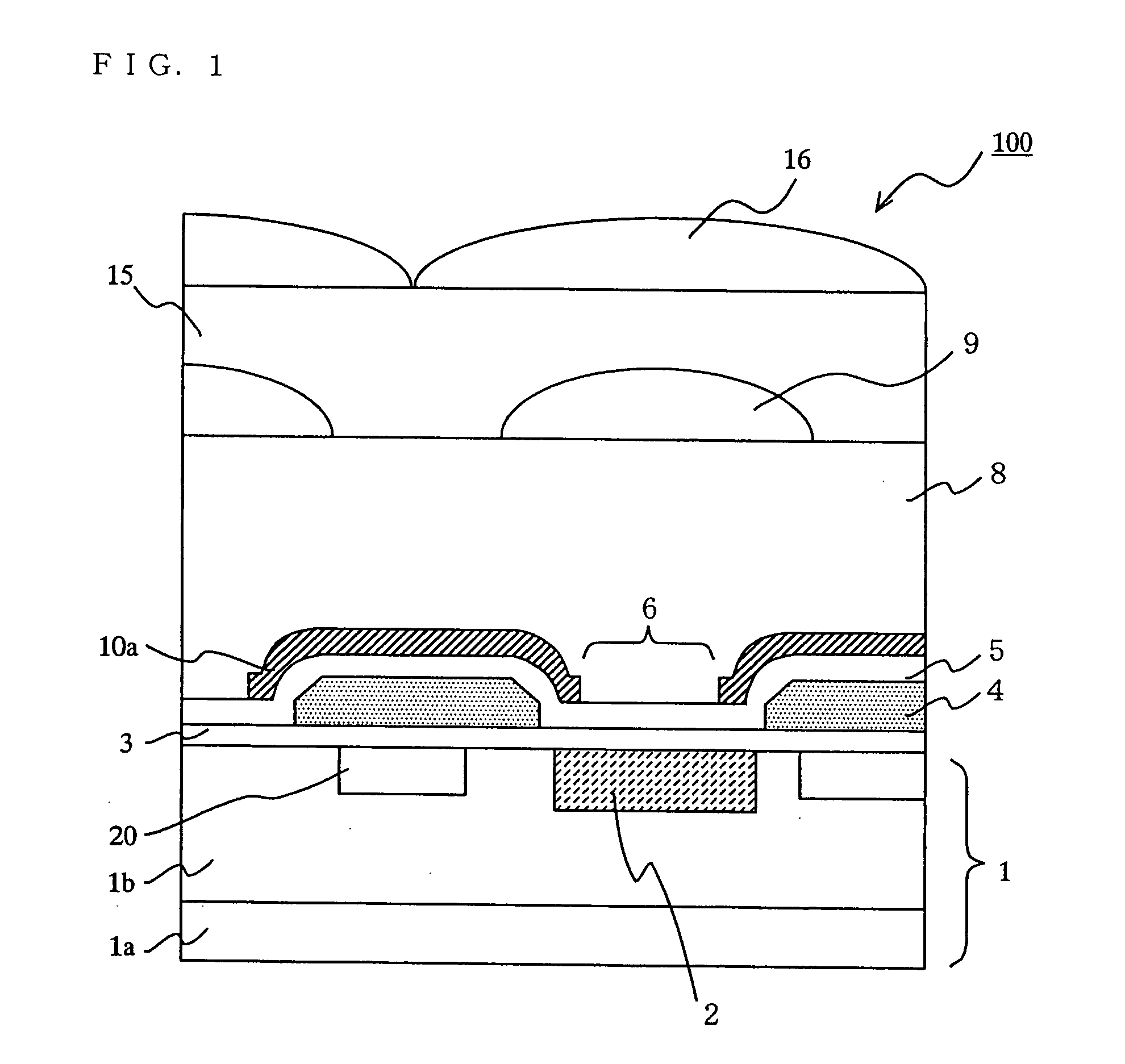
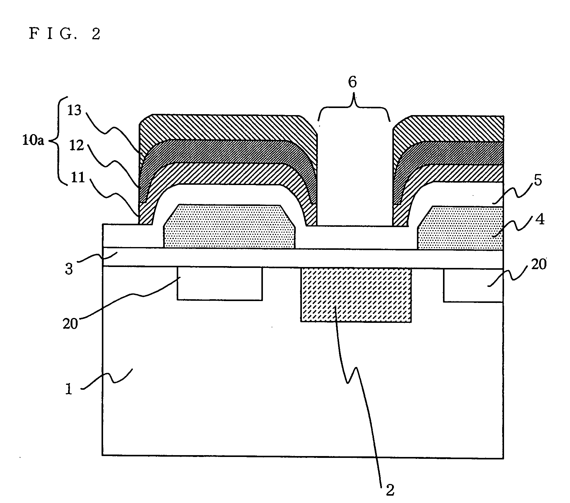
[0032]FIG. 1 shows an example of a cross-sectional structure of a commonly used solid-state imaging device. In a solid-state imaging device 100 shown in FIG. 1, a semiconductor substrate 1 is an epitaxial high-resistivity substrate in which an epitaxial layer 1b is formed on a main surface of a silicon substrate la by epitaxially growing a single crystal silicon layer. Photodiodes 2 of a conductivity type opposite to that of the epitaxial layer 1b are formed in a main surface of the semiconductor substrate 1 and generate charges in accordance with the intensity of received light. Charge transfer portions 20 are formed in the main surface of the semiconductor substrate 1 and transport charges that are generated in the photodiodes 2. Gate electrodes 4 are provided adjacent to each photodiode 2 on the semiconductor substrate 1 and serve as switches for moving the charges generated in the photodiodes 2 to the charge transfer portions 20. A light-shielding film 10a is formed so as to cov...

second embodiment

[0054]In this embodiment, a solid-state imaging device having a light-shielding film whose surface is formed of a high melting point metal silicide film, instead of the light-shielding film 10a whose surface is formed of the amorphous silicon film 13 of the first embodiment will be described. The solid-state imaging device of this embodiment has substantially the same structure as the solid-state imaging device 100 of the first embodiment, so that in the following, only different points will be described.

[0055]FIG. 6 shows a cross-sectional structure of a solid-state imaging device of the second embodiment of the present invention. In FIG. 6, the light-shielding film 10b is a film having a two-layered structure in which a tungsten-sputtered film 11, which is a high melting point metal film, and a tungsten silicide film 14, which is a high melting point metal silicide film, are laminated. The tungsten-sputtered film 11 serves as an adhesive layer for the tungsten silicide film 14. Th...

third embodiment

[0061]In this embodiment, a solid-state imaging device having a light-shielding film whose surface is formed of a high melting point metal silicide film having a three-layered structure, instead of the light-shielding film 10b having a two-layered structure of the second embodiment will be described. The second embodiment is different from the third embodiment in the number of films constituting the light-shielding film, and therefore in the following, only different points will be described.

[0062]FIG. 7 shows a cross-sectional structure of a solid-state imaging device of the third embodiment of the present invention. In FIG. 7, the light-shielding film 10c is a film having a three-layered structure in which a tungsten-sputtered film 11, and a tungsten CVD film 12, which are high melting point metal films, and a tungsten silicide film 14, which is a high melting point metal silicide film, are laminated. The tungsten-sputtered film 11 serves as an adhesive layer for the tungsten CVD ...


PUM

PropertyMeasurementUnit
thicknessaaaaaaaaaa
thicknessaaaaaaaaaa
temperatureaaaaaaaaaa

Abstract

In a solid-state imaging device, a light-shielding film 10a is formed of at least one of a high melting point metal film or a high melting point metal compound film. The surface of the light-shielding film 10a is constituted by an amorphous silicon film 13. Instead of the amorphous silicon film 13, the surface of the light-shielding film may be covered with any one of a high melting point metal film containing silicon, a high melting point metal silicide film and an oxide film. Thus, the adherence between the light-shielding film 10a and the resist can be increased and the resist can be prevented from being peeled from the light-shielding film, and thus a solid-state imaging device with a high yield even with small pixels and a method for producing the same can be provided.

Description

BACKGROUND OF THE INVENTION[0001]1. Field of the Invention[0002]The present invention relates to a solid-state imaging device and a method for producing the same. More specifically, the present invention relates to a light-shielding film constituting pixels and a method for producing the same.[0003]2. Description of the Background Art[0004]In recent years, a demand for solid-state imaging devices has been increased, and the number of pixels has been increased while the size of a pixel has been increasingly reduced. In general, the pixels of a solid-state imaging device are provided with a light-shielding film in order to prevent light from falling on a portion other than a light-receiving area, and an opening through which light enters the light-receiving area is formed in a portion of the light-shielding film (e.g., Japanese Laid-Open Patent Publication No. 10-284710).[0005]Hereinafter, a conventional solid-state imaging device will be described with reference to FIG. 9. FIG. 9 is ...

Claims


Application Information

Patent Timeline
Patent Type & Authority Applications(United States)
IPC IPC(8): H01L21/00H01L27/14H01L27/148
CPCH01L27/14623H01L27/14685H01L27/14627H01L27/14625
Inventor YANO, TOSHIHIKODOI, HITOSHINIISOE, NAOTO
Owner PANASONIC SEMICON SOLUTIONS CO LTD
Why Eureka
Try Eureka