Touch display panel

a touch display panel and display panel technology, applied in the field of touch display panels, can solve the problems of complicated manufacturing processes of the touch display panel, the inability to reduce the entire thickness of the finished product, etc., and achieve the effect of simplifying the complicated manufacturing process of the conventional touch display panel

Active Publication Date: 2011-11-08
CHUNGHWA PICTURE TUBES LTD
View PDF12 Cites 4 Cited by
  • Summary
  • Abstract
  • Description
  • Claims
  • Application Information

AI Technical Summary

Benefits of technology

[0008]The present invention is directed to a touch display panel for simplifying complicated manufacturing processes of a conventional touch display panel.
[0015]In the present invention, the color filter patterns are piled to form the touch points, and therefore it is not necessary to additionally form touch points in the touch display panel of the present invention. Namely, in the touch display panel of the present invention, the color filter patterns for display and the touch points are fabricated simultaneously, so as to simplify the manufacturing processes of the entire touch display panel. Moreover, in the touch display panel of the present invention, color filter layers can be piled to form the spacers of the touch panel, so as to ensure that a gap exists in the touch panel. As such, the color filter patterns, the touch points, and the spacers in the touch display panel of the present invention can be fabricated at the same time, thus simplifying the manufacturing processes.

Problems solved by technology

However, with said design, the entire thickness of the finished product cannot be reduced.
Nonetheless, the spacers must be additionally scattered or manufactured, which complicates manufacturing processes of the touch display panel.

Method used


Image

  • Touch display panel
  • Touch display panel
  • Touch display panel

Examples


Embodiment Construction

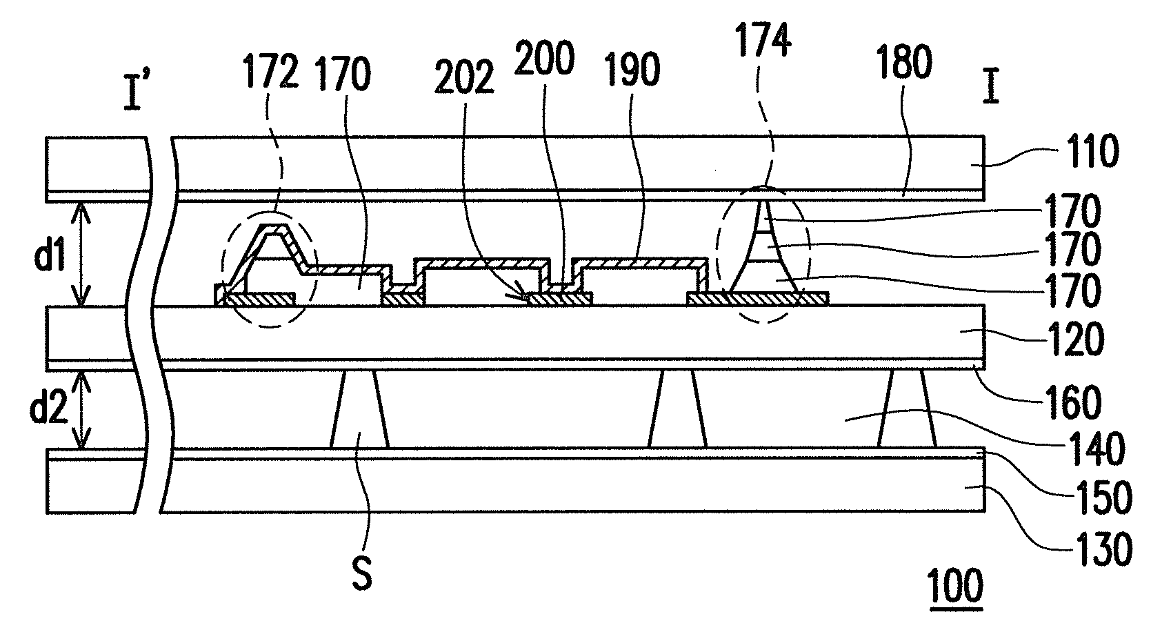
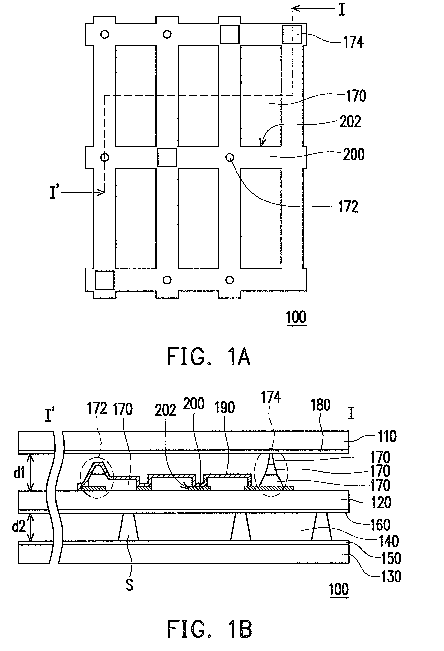
[0021]FIG. 1A is a schematic top view of a touch display panel according to an embodiment of the present invention. FIG. 1B is a cross-sectional view taken along a section line I-I′ depicted in FIG. 1A. Referring to FIGS. 1A and 1B, a touch display panel 100 includes a first substrate 110, a second substrate 120, a third substrate 130, a liquid crystal layer 140, a pixel array 150, an opposite electrode 160, a plurality of color filter patterns 170, a first sensing electrode 180, and a second sensing electrode 190. The first substrate 110, the second substrate 120, and the third substrate 130 are disposed in parallel. The second substrate 120 is disposed between the first substrate 110 and the third substrate 130. The liquid crystal layer 140 is disposed between the second substrate 120 and the third substrate 130. The pixel array 150 is disposed between the liquid crystal layer 140 and the third substrate 130. The opposite electrode 160 is disposed between the liquid crystal layer ...


PUM


Abstract

A touch display panel includes a first substrate, a second substrate, a third substrate, a liquid crystal layer disposed between the second and the third substrates, a pixel array disposed between the liquid crystal layer and the third substrate, an opposite electrode, color filter patterns, a first sensing electrode, and a second sensing electrode. The first, the second, and the third substrates are disposed in parallel. The color filter patterns and the opposite electrode that are disposed between the liquid crystal layer and the second substrate are respectively disposed on opposite sides of the second substrate. Some color filter patterns are piled to form touch points. The first sensing electrode on the first substrate faces the second substrate. The second sensing electrode covers the touch points and some color filter patterns. A height of the touch points is less than a gap between the first and the second substrates.

Description

CROSS-REFERENCE TO RELATED APPLICATION[0001]This application claims the priority benefit of Taiwan application serial no. 97141642, filed on Oct. 29, 2008. The entirety of the above-mentioned patent application is hereby incorporated by reference herein and made a part of specification.BACKGROUND OF THE INVENTION[0002]1. Field of the Invention[0003]The present invention relates to a touch display panel, and more particularly to a touch display panel in which touch points are not required to be additionally disposed.[0004]2. Description of Related Art[0005]Information technologies (ITs), wireless mobile communications, and information home appliances have been rapidly developed and widely applied in recent years. To meet current demands on portable, compact, and user-friendly IT products, touch panels have been introduced as input devices in replacement of conventional input devices, such as keyboards or mice. Besides, to increase dimensions of display screens and facilitate touch co...

Claims


Application Information

Patent Timeline
Patent Type & Authority Patents(United States)
IPC IPC(8): G06F3/041
CPCG06F3/0412G06F3/047
Inventor HUANG, KUEI-WEI
Owner CHUNGHWA PICTURE TUBES LTD
Why Eureka
Try Eureka