Semiconductor device

a technology of semiconductor devices and semiconductors, applied in semiconductor devices, semiconductor/solid-state device details, electrical apparatus, etc., can solve the problems of affecting the operation speed of the device, the actual high or low state is erroneously read, and the operation speed cannot be made faster, etc., to achieve high density and integration, low cost, and high efficiency.

Inactive Publication Date: 2005-01-13
RENESAS ELECTRONICS CORP
View PDF24 Cites 3 Cited by
  • Summary
  • Abstract
  • Description
  • Claims
  • Application Information

AI Technical Summary

Benefits of technology

[0008] In consideration of the foregoing problem, it is an object of the present invention to provide a semiconductor device which contains a lower inductance of the wiring system for the purpose of meeting with the requests of high density and integration, low cost and the like without making the manufacturing process complicated as well as making the semiconductor device operate at a faster clock frequency than several hundreds MHz as keeping its noise low. Further, the present invention provides a capability of reducing the noises generated on the power wiring side as well as the ground wiring side. Moreover, the invention also provides the solving method for a general structure having difficulty in reducing the inductance on the wiring system because of the pads and bumps located on the chip surface.

Problems solved by technology

However, those semiconductor devices still have a problem in speed.
If this kind of noise appears in the power supply, the ground or the signal line, the actual high or low state is erroneously read.
This may lead to malfunction.
Hence, in order to reduce the operating frequency, the operation speed cannot be made faster.
However, considering that a conductor having a length of several millimeters contains roughly several nH inductance, the foregoing semiconductor does not provide so low an inductance as meeting the request by the recent various systems that need to operate at a quite fast speed.
However, it does not consider reduction of the inductance on the ground wiring side.
Hence, the semiconductor device has no means of reducing the noise caused on the ground wiring side.
It means that the planar conductive layer cannot be easily formed.

Method used


Image

  • Semiconductor device
  • Semiconductor device
  • Semiconductor device

Examples


Embodiment Construction

[0040] Hereafter, the embodiments of the present invention will be described with reference to the appended drawings.

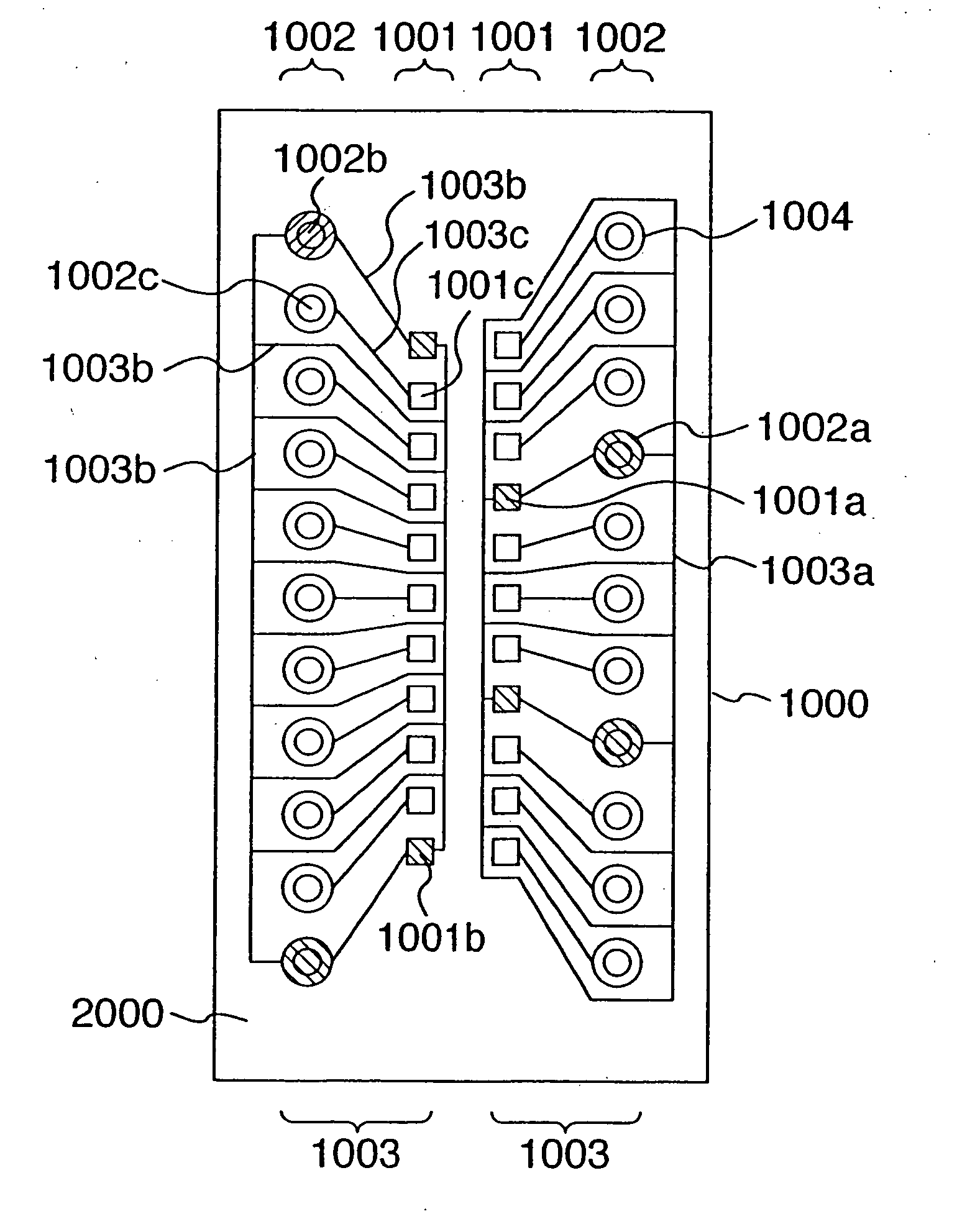
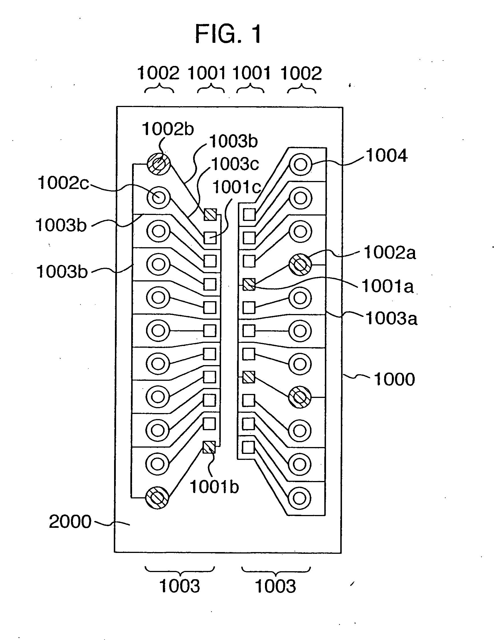
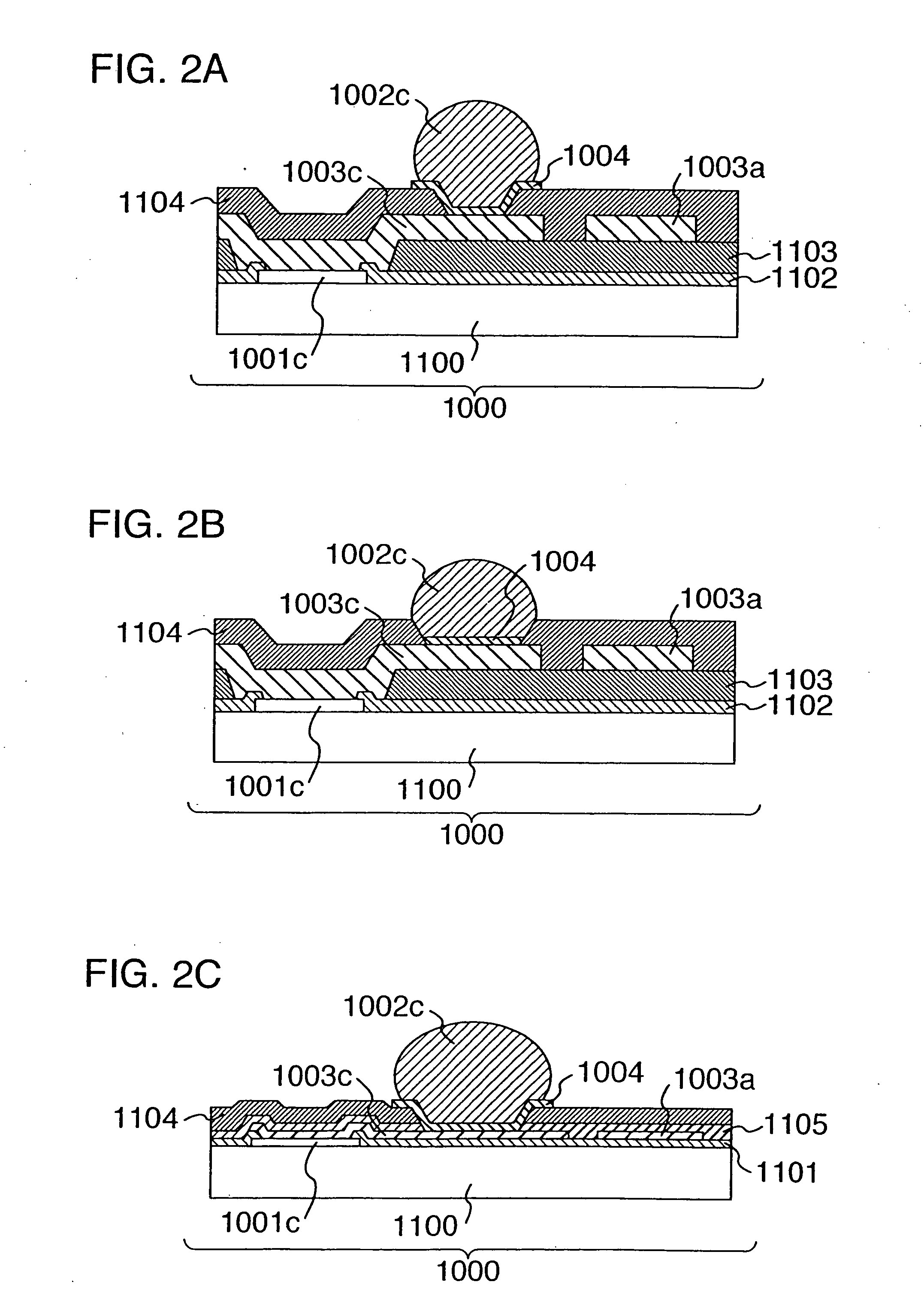
[0041]FIG. 1 is a plan view showing a pad forming surface of a semiconductor device according to a first embodiment of the present invention. A semiconductor device 1000 is made up of a semiconductor element 1100 composed of a roughly rectangular silicon chip having sides of several millimeters or several tens millimeters as shown in the section of FIGS. 2A, 2B, 2C, a plurality of pads 1001, a bump forming section 1004, a plurality of bumps 1002, a plurality of wiring sections 1003 for connecting them formed on a pad forming surface 2000 of the semiconductor element 1100. The pads 1001 are further divided into power pads 1001a, ground pads 1001b and signal pads 1001c. The power bumps 1002a are further divided into ground bumps 1002b and signal bumps 1002c. The power wiring sections 1003a are further divided into ground wiring sections 1003b and signal wiring sections...


PUM


Abstract

A semiconductor device including a semiconductor element having external terminals at a first level and external electrodes at a second level, higher than the first level. The external terminals include power terminals, ground terminals and signal terminals formed on a main surface of the semiconductor element. The external electrodes include power electrodes connected to the power terminals via power connecting sections, ground electrodes connected to the ground terminals via ground connecting sections and signal electrodes connected to the signal terminals via signal connecting sections. One of the signal terminals, signal electrodes and corresponding signal connecting sections are surrounded by either the power connecting sections connecting the power terminals and power electrodes or by the ground connection sections connecting the ground terminals and ground electrodes.

Description

BACKGROUND OF THE INVENTION [0001] The present invention relates to a semiconductor device which is structured to connect pads with bumps for outside connection by wiring sections in a semiconductor element and more particularly to the semiconductor device which may reduce the operating noise even if its clock frequency is several hundred MHz or more. [0002] In recent days, semiconductor devices have been more and more requested to enhance its density, integration and speed and lower its cost. In order to meet with the request, for example, as disclosed in JP-A-8-250498, a semiconductor device has been designed so that wiring sections and bumps are formed on a pad forming surface of a semiconductor element and those wiring sections and bumps are conductive with the pads. As shown in FIG. 17, in such a technology, a pad forming surface of a semiconductor element is formed to have a plurality of pads, and a plurality of wiring sections are formed on the pad forming surface so that tho...

Claims


Application Information

Patent Timeline
Patent Type & Authority Applications(United States)
IPC IPC(8): H01L21/60H01L21/3205H01L21/822H01L23/50H01L23/52H01L23/552H01L23/64H01L23/66H01L27/04H01L27/14
CPCH01L23/50H01L23/5286H01L24/13H01L2924/10253H01L2924/014H01L23/552H01L23/645H01L23/66H01L24/10H01L2224/13099H01L2224/16H01L2924/01004H01L2924/01013H01L2924/01029H01L2924/01033H01L2924/01074H01L2924/01077H01L2924/01079H01L2924/01082H01L2924/19041H01L2924/30105H01L2924/30107H01L2924/3025H01L2924/01005H01L2924/01006H01L2924/01023H01L2924/01024H01L2924/00H01L2924/12042H01L2224/05571H01L2924/14H01L2224/13H01L2224/05001H01L2224/05569H01L2224/05024H01L2224/05008H01L2224/05022H01L2224/05572H01L2224/06135H01L24/05H01L2224/023H01L2924/00012H01L2924/0001H01L21/822H01L27/14H01L21/60
Inventor SHIMIZU, HIROYANISHIMURA, ASAOMIYAMOTO, TOSHIHOTANAKA, HIDEKIMIURA, HIDEO
Owner RENESAS ELECTRONICS CORP
Why Eureka
Try Eureka