Touch element and touch display module

a touch element and display module technology, applied in the field of electronic elements and display modules, can solve the problems of complex manufacturing process of capacitive touch elements and difficult reduction of manufacturing costs, and achieve the effect of losing manufacturing costs

Active Publication Date: 2017-10-24
HANNSTOUCH SOLUTION
View PDF14 Cites 3 Cited by
  • Summary
  • Abstract
  • Description
  • Claims
  • Application Information

AI Technical Summary

Benefits of technology

[0006]In the conventional technology, a capacitive touch element includes a plurality of first sensing series extending along a direction and a plurality of second sensing series extending along another direction. A plurality of insulating patterns are disposed at positions where the first sensing series and the second sensing series are overlapped, so that the first and second sensing series do not result in a short circuit. However, under such configuration, a sensing array of the capacitive touch element formed of the first sensing series and the second sensing series requires several processes to be completely manufactured. Thus, the manufacturing process of the capacitive touch element is complicated and the manufacturing cost thereof is difficult to reduce.

Problems solved by technology

However, under such configuration, a sensing array of the capacitive touch element formed of the first sensing series and the second sensing series requires several processes to be completely manufactured.
Thus, the manufacturing process of the capacitive touch element is complicated and the manufacturing cost thereof is difficult to reduce.

Method used


Image

  • Touch element and touch display module
  • Touch element and touch display module
  • Touch element and touch display module

Examples


first embodiment

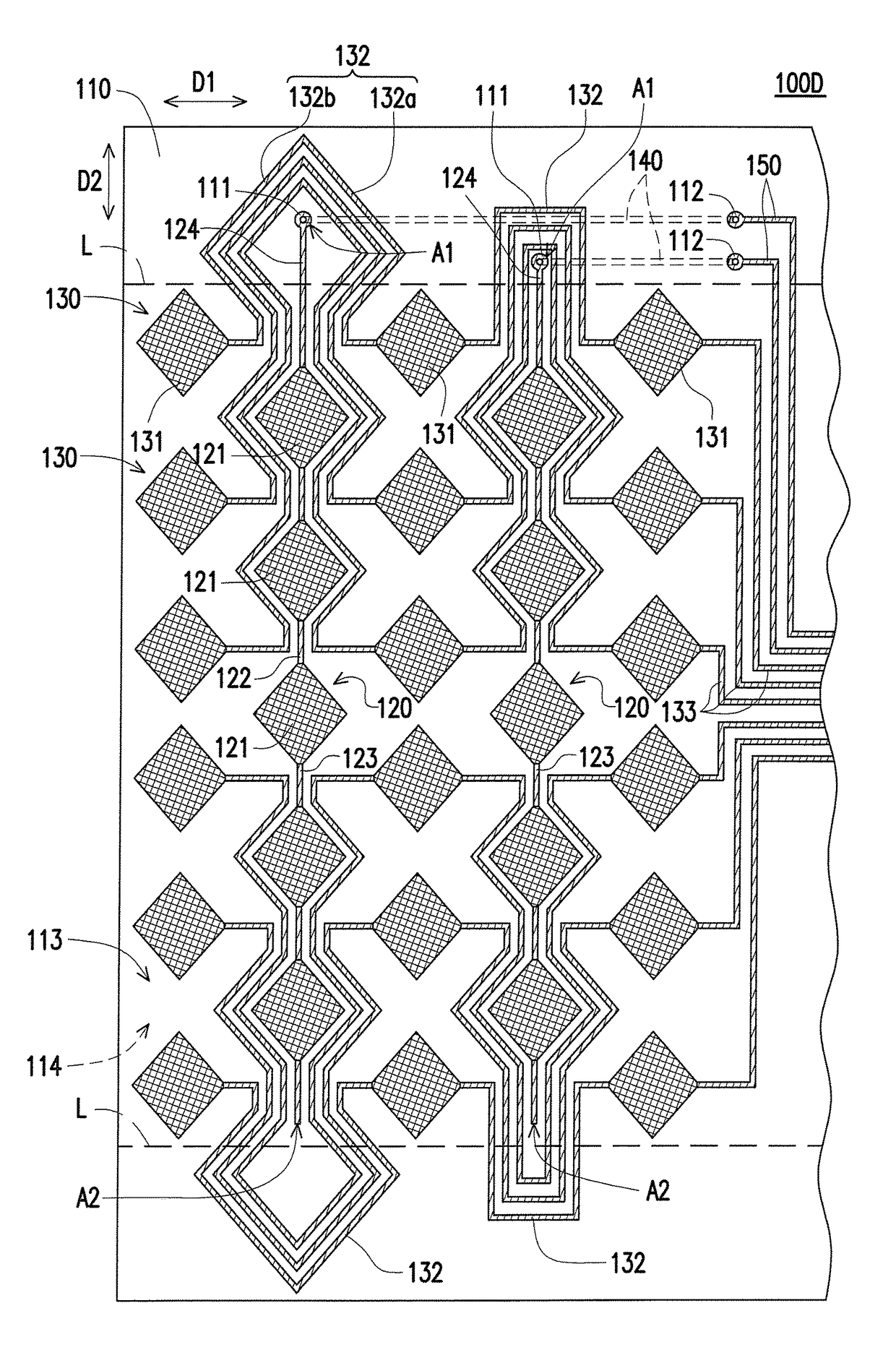
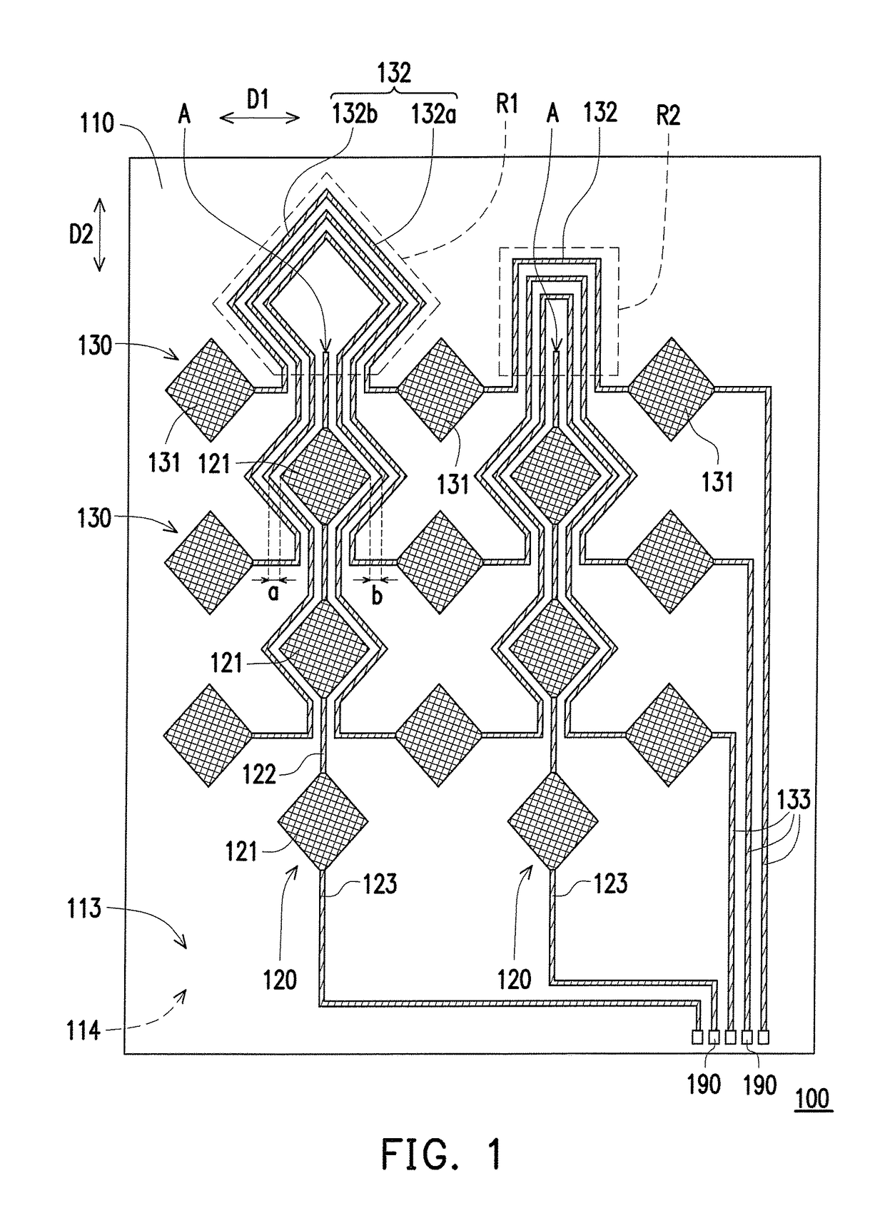
[0019]FIG. 1 is a top view illustrating a touch element according to the invention. Referring to FIG. 1, in this embodiment, a touch element 100 is a single-layer touch panel, for example. The touch element 100 includes a substrate 110, a plurality of first sensing series 120 separated from each other and a plurality of second sensing series 130 separated from each other, and the plurality of first sensing series 120 and the plurality of second sensing series 130 do not overlap with each other. The substrate 110 is a flexible substrate or a rigid substrate, for example, has a first surface 113 and a second surface 114 opposite to the first surface 113. In general, a material of the flexible substrate may include polyimide (PI), polyethylene terephthalate (PET), polyethylene naphthalate (PEN), polyether sulfone (PES), polymethyl methacrylate (PMMA), polycarbonate (PC), or metal foil. A material of the rigid substrate may include glass, quartz, or acrylics.

[0020]The first sensing seri...

second embodiment

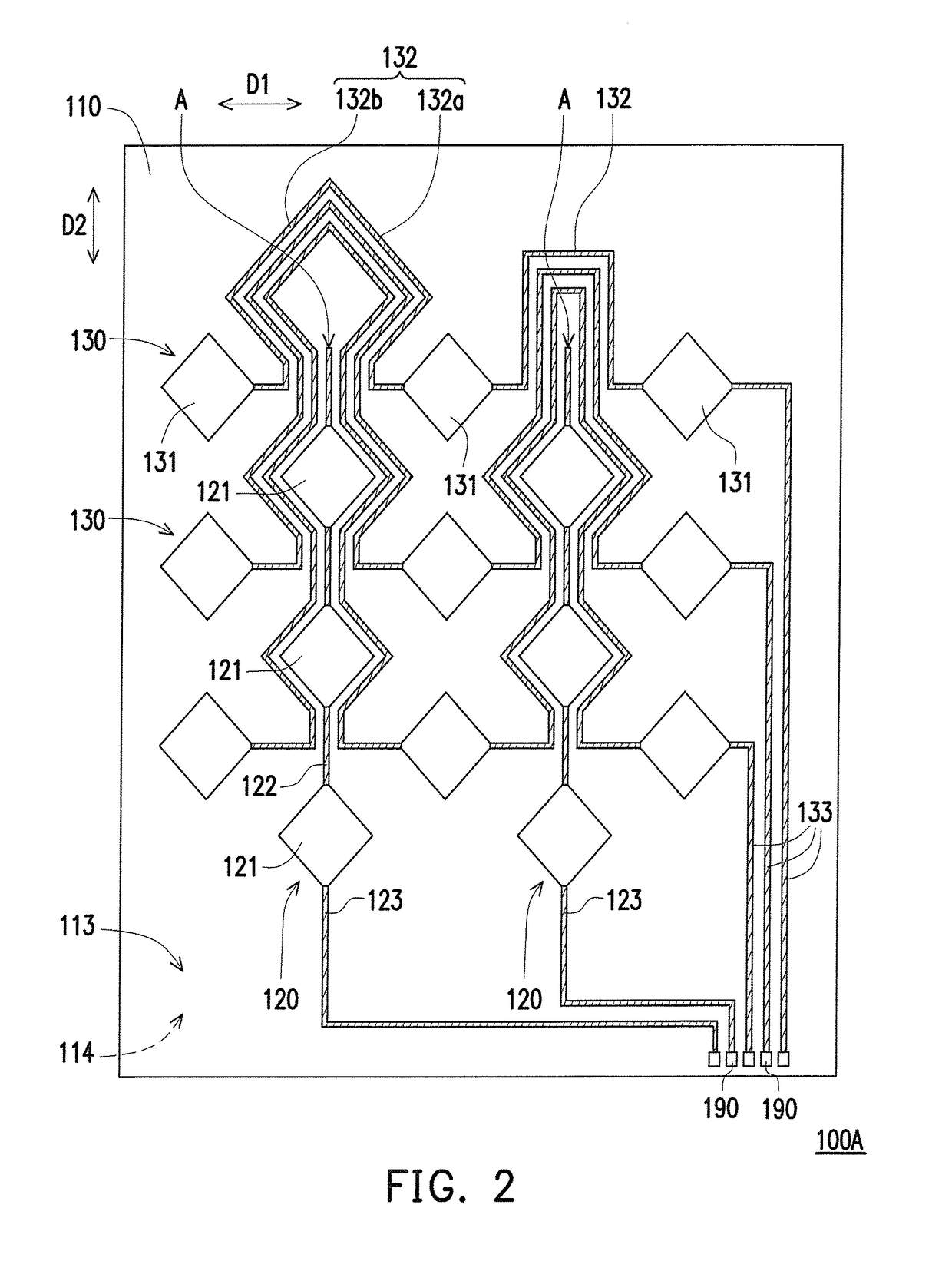
[0026]FIG. 2 is a top view illustrating a touch element according to the invention. Referring to FIG. 2, a touch element 100A of FIG. 2 is substantially similar to the touch element 100 shown in FIG. 1, except for a difference that materials the first sensing pads 121 and the second sensing pads 131 of this embodiment may include transparent conductive oxide, such as ZnO, In2O3, SnO2, ITO, AZO, GZO, IGZO, or ZTO, and the materials of the bridging lines 122, the connection lines 132, and the wirings 123 and 133 may still include metal.

[0027]In other words, based on the manufacturing requirements, the first sensing pads and the second sensing pads of the touch element according to the embodiments of the invention may be formed of metal mesh or transparent conductive oxide. In general, the lines on the substrate are mostly formed of conductive metal or alloy. However, the invention is not limited thereto. In another embodiment, the materials of the first sensing pads 121, the second se...

fourth embodiment

[0032]FIG. 4 is a top view illustrating a touch element according to the invention. Referring to FIG. 4, a touch element 100C shown in FIG. 4 is substantially similar to the touch element 100, except for a difference that the touch element 100C further includes a flexible circuit board 160. The flexible circuit board 160 is disposed on the first surface 113 of the substrate 110. Namely, the flexible circuit board 160 is disposed on a side of the substrate 110 where the first sensing series 120 and the second sensing series 130 are disposed.

[0033]More specifically, the flexible circuit board 160 is located at terminals of the first sensing series 120, and is directly attached to the substrate 110. A patterned circuit 180 is disposed on the flexible circuit board 160. In addition, the flexible circuit board 160 is attached to the first surface 113 of the substrate 110 with a side where the patterned circuit 180 is disposed, for example. In this way, the patterned circuit 180 is electr...


PUM


Abstract

A touch sensing device including a substrate, a plurality of first sensing series separated from each other and a plurality of second sensing series separated from each other is provided. The substrate has a first surface and a second surface. The first sensing series are disposed on the first surface. Each of the first sensing series includes a plurality of first sensing pads connected to each other. The second sensing series are disposed on the first surface. Each of the second sensing series includes a plurality of second sensing pads distributed between the first sensing series and a plurality of connection lines connecting the second sensing pads. Each of the connection lines extends along an edge of one of the first sensing series, and each of the connection lines is electrically connected to the second sensing pads located at two opposite sides of the first sensing series.

Description

CROSS-REFERENCE TO RELATED APPLICATION[0001]This application claims the priority benefit of Chinese application serial no. 201510564681.9, filed on Sep. 8, 2015. The entirety of the above-mentioned patent application is hereby incorporated by reference herein and made a part of this specification.BACKGROUND OF THE INVENTION[0002]1. Field of the Invention[0003]The invention relates to an electronic element and a display module, and particularly relates to a touch element and a touch display module.[0004]2. Description of Related Art[0005]Many electronic devices (e.g., cell phones, tablet computers, etc.,) are configured with touch elements, so as to make the operating interfaces thereof more user friendly. Generally speaking, based on the sensing methods, the touch elements may be divided into capacitive touch elements, resistive touch elements, surface acoustic wave touch elements, and infrared touch elements. Due to its outstanding sensitivity, the capacitive touch elements are bro...

Claims


Application Information

Patent Timeline
Patent Type & Authority Patents(United States)
IPC IPC(8): G06F3/041G06F3/044
CPCG06F3/0412G06F3/0416G06F3/044G06F2203/04111G06F3/04164G06F3/0443G06F3/0446
Inventor LO, WEI-JENHUANG, HUNG-YI
Owner HANNSTOUCH SOLUTION
Why Eureka
Try Eureka