Semiconductor device and manufacturing method thereof

a technology of semiconductor devices and semiconductors, applied in semiconductor devices, load-engaging elements, transistors, etc., can solve the problems of large dispersion capacity and deterioration of element isolation ability, and achieve the effect of improving the degree of integration, increasing the number of process steps, and easy and sure improvemen

Inactive Publication Date: 2007-07-19
FUJITSU SEMICON LTD +1
View PDF8 Cites 4 Cited by
  • Summary
  • Abstract
  • Description
  • Claims
  • Application Information

AI Technical Summary

Benefits of technology

[0013] The present invention is made in consideration of the above-stated problems, and an object thereof is to provide a semiconductor device and a manufacturing method thereof enabling to form a channel stop region at a desired portion under respective STI structures having different insulator thicknesses, and to easily and certainly realize a further improvement in a degree of integration in a semiconductor memory, without incurring an increase of process steps and a complication of a manufacturing process.

Problems solved by technology

Recently, further improvement in a degree of integration is required in a semiconductor memory, and a configuration described in the Patent Document 1 and so on becomes inadequate to comply the request.
The channel stop region 103 is too deep under the STI structure 102, and therefore, there is a problem that the substrate concentration immediately under the STI structure 102 becomes thin to cause a deterioration of the element isolation ability.
A substantial film thickness of the capacitor insulating film increases by an enhanced oxidation originated in the above, then a desired and designed value of capacity cannot be obtained because a capacity value becomes a small value, and a problem occurs in which a dispersion of the capacity becomes large.

Method used


Image

  • Semiconductor device and manufacturing method thereof
  • Semiconductor device and manufacturing method thereof
  • Semiconductor device and manufacturing method thereof

Examples


Embodiment Construction

[0027] -Basic Gist of Present Invention-

[0028] The present inventor studied hard to solve the above-stated problems, and as a result, the inventor comes up with a technical idea to form a channel stop region efficiently without incurring an increase of process steps and a complication of a manufacturing process, by positively applying an impurity doping for a threshold voltage adjustment of a transistor structure.

[0029] A method to be a preliminary step of the idea is explained for describing the present invention in detail.

[0030] The present inventor firstly examined a forming method of an isolation / consolidation type capacitor structure as described under.

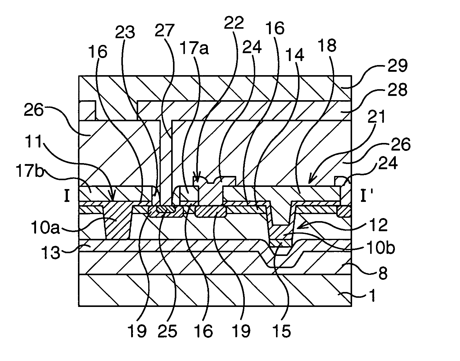
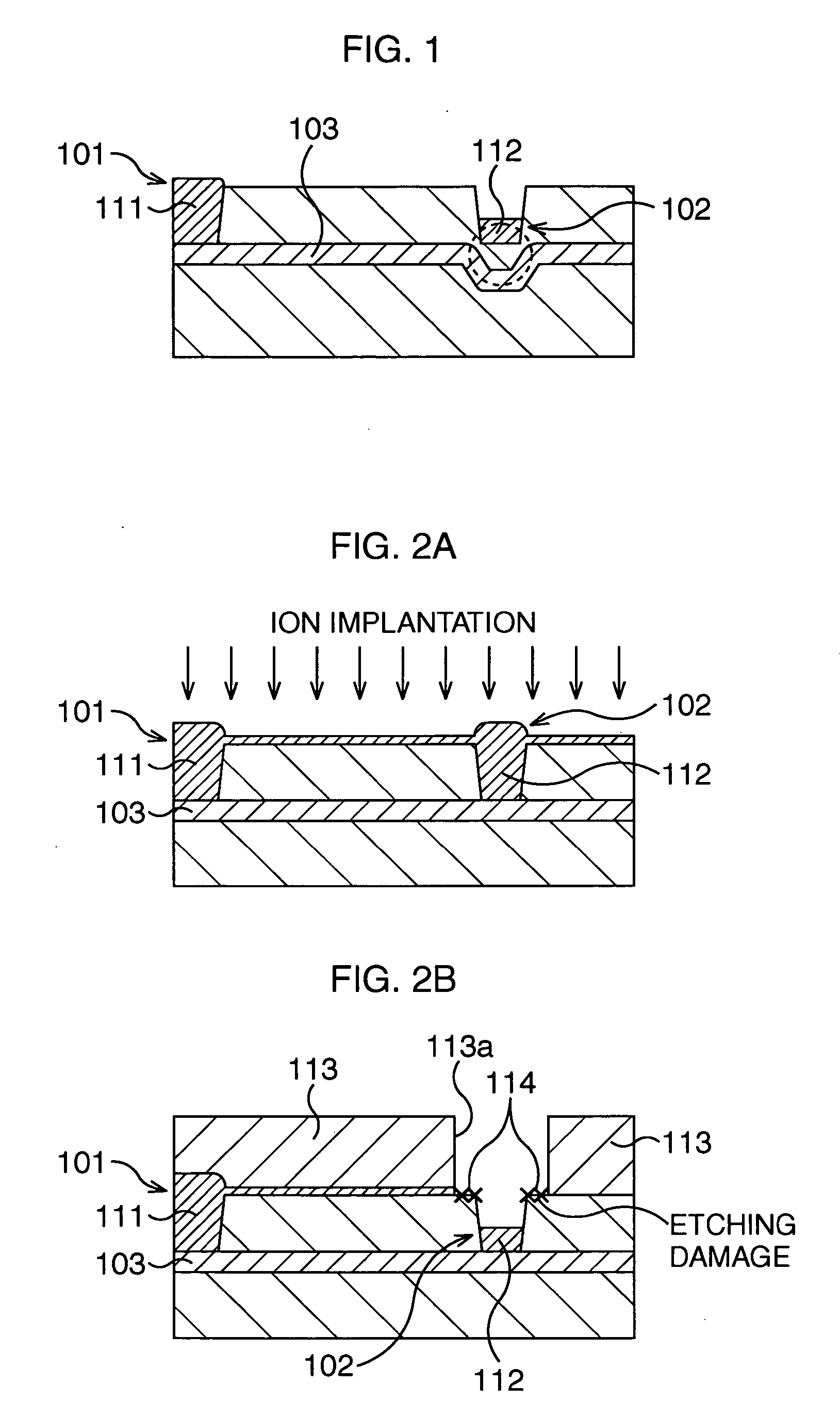
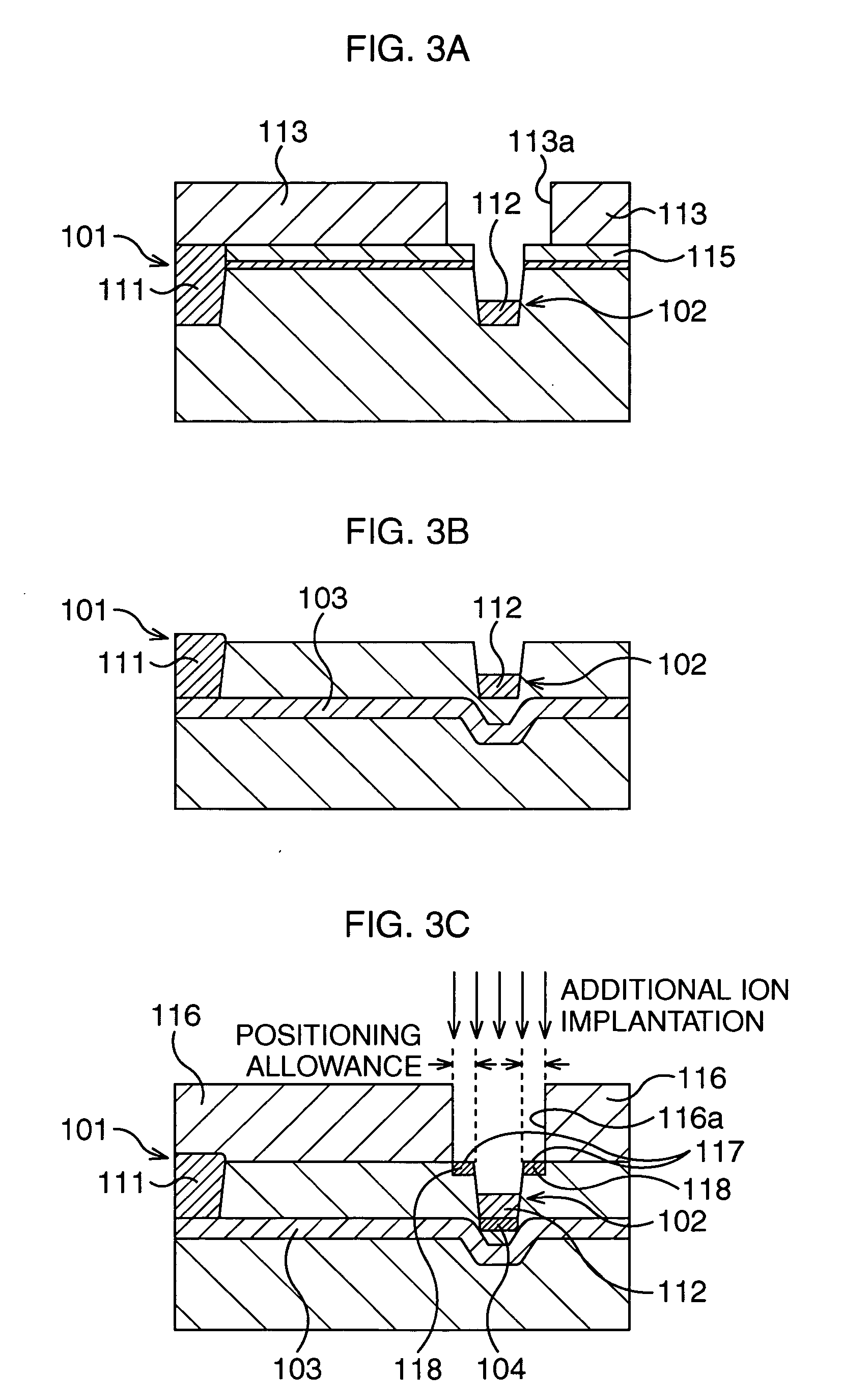
[0031] At first, a surface layer of an insulating film 112 is etched by using a resist mask 113 under a state of forming a protective film 115 such as a silicon nitride film so as not to give an etching damage to a semiconductor substrate, as shown in FIG. 3A.

[0032] Subsequently, the resist mask 113 and the protective film 1...


PUM


Abstract

A channel stop region is formed immediately under an STI, and thereafter, an ion implantation is performed with conditions in which an impurity is doped into an upper layer portion of an active region, and at the same time, the impurity is also doped into immediately under another STI, and a channel dose region is formed at the upper layer portion of the active region, and another channel stop region is formed immediately under the STI.

Description

CROSS-REFERENCE TO RELATED APPLICATIONS [0001] This application is based upon and claims the benefit of priority from the prior Japanese Patent Application No. 2005-340869, filed on Nov. 25, 2005, the entire contents of which are incorporated herein by reference. BACKGROUND OF THE INVENTION [0002] 1 Field of the Invention [0003] The present invention relates to a semiconductor device and a manufacturing method thereof including STI structures, and in particular, it is intended for a semiconductor memory including a transistor structure and a capacitor structure in a memory cell region. [0004] 2 Description of the Related Art [0005] In a semiconductor memory device having memory cells taking a constitution storing a data into a capacitor structure, various device configurations are thought out whose objects are to reduce a memory cell area and to improve a degree of integration. In particular, when so-called an STI (Shallow Trench Isolation) structure is used as an element isolation ...

Claims


Application Information

Patent Timeline
Patent Type & Authority Applications(United States)
IPC IPC(8): H01L21/8242
CPCH01L21/84H01L27/10805H01L29/94H01L27/10873H01L27/12H01L27/1085H10B12/03H10B12/30H10B12/05B66C1/06B66C13/20
Inventor ASANO, MASAYOSHISUZUKI, YOSHIYUKI
Owner FUJITSU SEMICON LTD
Why Eureka
Try Eureka