Imaging device

a technology of imaging device and manufacturing process, which is applied in the direction of radioation controlled devices, television system scanning details, television system, etc., can solve the problems of complicated manufacturing process, and increasing the manufacturing cost of imaging device, so as to speed up the signal processing unit, improve the performance of sensor units, and improve the effect of sensor performan

Active Publication Date: 2016-03-03
NIKON CORP
View PDF2 Cites 2 Cited by
  • Summary
  • Abstract
  • Description
  • Claims
  • Application Information

AI Technical Summary

Benefits of technology

[0007]However, with the configuration (single-chip configuration) having the function of the signal processing chip such as an A / D converter provided within the sensor chip, there is a difference between the manufacturing process suitable for improving the performance of the sensor unit such as the pixel array and the manufacturing process suitable for speeding up the signal processing unit such as an A / D converter, which makes the manufacturing process of imaging devices complicated. For example, the dynamic range is expanded in the sensor unit by raising the driving voltage (power supply voltage), and the influence of noise is reduced. In contrast, high-speed operation is realized in the signal processing unit by operating microscopic transistors at a low power supply voltage. Therefore, a complicated process control is required to manufacture, on a single chip, a sensor unit which operates at a high power supply voltage and a signal processing unit using a microscopic transistor which operates at a low power supply voltage, thereby making the manufacturing process complicated. Accordingly, the manufacturing cost of the imaging device increases.
[0008]Note that, when the sensor unit and the signal processing unit are manufactured on a single chip through the use of the manufacturing process suitable for one of the sensor unit and the signal processing unit in order to reduce the manufacturing cost, performance of the imaging device decreases. For example, the use of a manufacturing process which gives a higher priority to improving the performance of the sensor unit results in insufficient miniaturization of transistors of the signal processing unit, which may lead to an increased area of the signal processing unit and increased power consumption. Alternatively, the use of a manufacturing process which gives a higher priority to miniaturization of transistors of the signal processing unit results in a narrower dynamic range because the pressure resistance of transistors or the like of the sensor unit becomes lower.

Problems solved by technology

However, with the configuration (single-chip configuration) having the function of the signal processing chip such as an A / D converter provided within the sensor chip, there is a difference between the manufacturing process suitable for improving the performance of the sensor unit such as the pixel array and the manufacturing process suitable for speeding up the signal processing unit such as an A / D converter, which makes the manufacturing process of imaging devices complicated.
Therefore, a complicated process control is required to manufacture, on a single chip, a sensor unit which operates at a high power supply voltage and a signal processing unit using a microscopic transistor which operates at a low power supply voltage, thereby making the manufacturing process complicated.
Accordingly, the manufacturing cost of the imaging device increases.
For example, the use of a manufacturing process which gives a higher priority to improving the performance of the sensor unit results in insufficient miniaturization of transistors of the signal processing unit, which may lead to an increased area of the signal processing unit and increased power consumption.

Method used


Image

  • Imaging device
  • Imaging device
  • Imaging device

Examples


Embodiment Construction

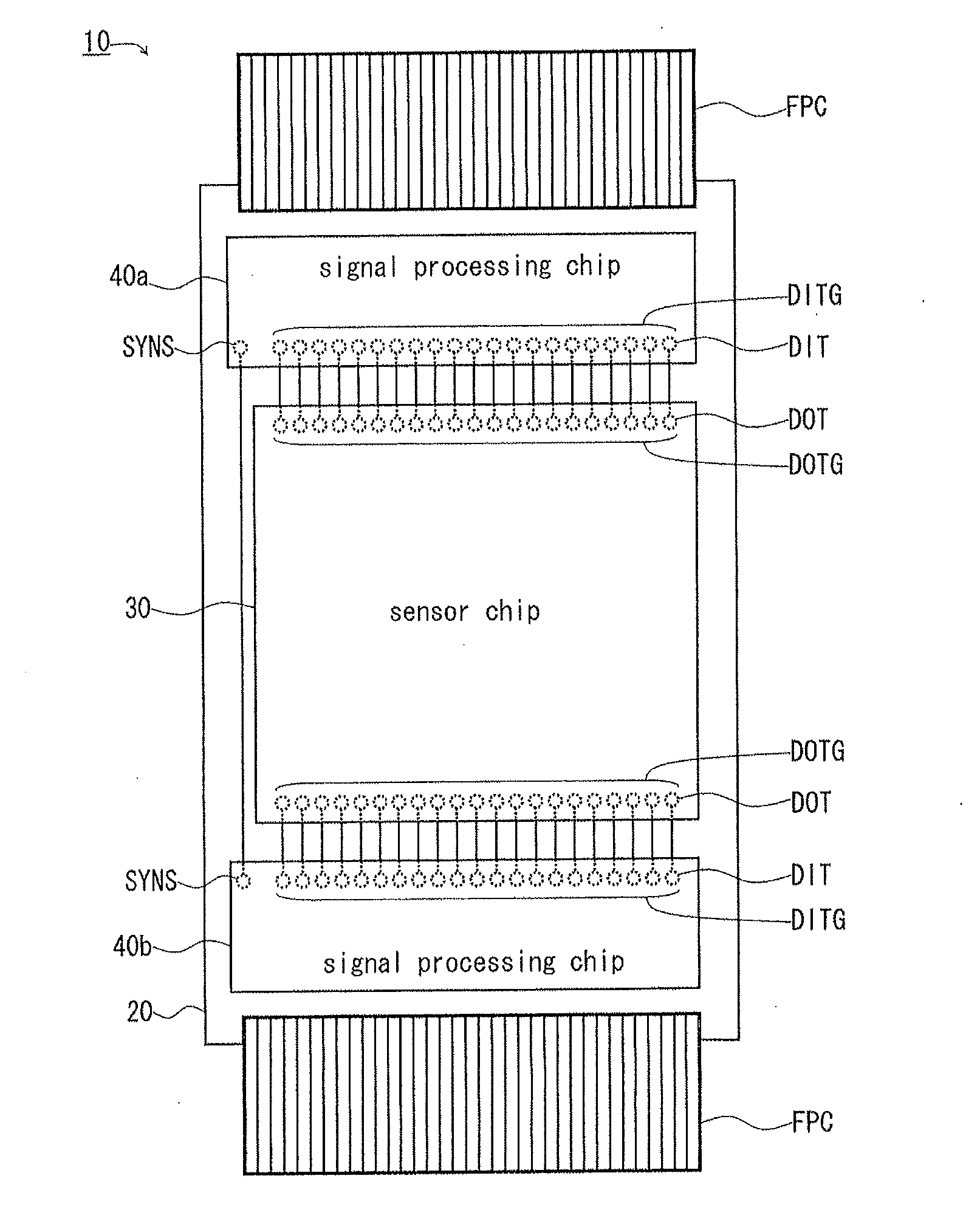
[0019]In the following, embodiments of the present invention will be described using the drawings. Some of the signal, signal line, and terminal in the drawings collectively show a plurality of such components. For example, in the following explanation, a plurality of control signals for controlling the driving timing of a sensor chip 30 is collectively referred to as a driving control signal CNTP.

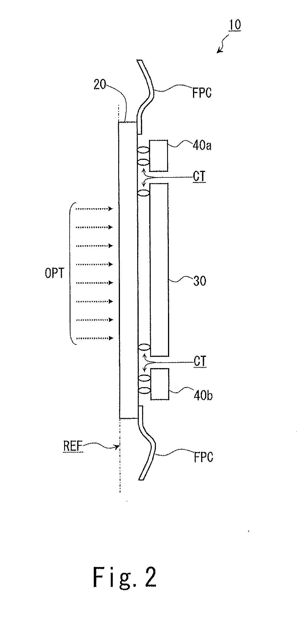
[0020]FIG. 1 shows an embodiment of the present invention. Note that FIG. 1 shows the overall imaging device 10 seen from the other side of the incidence plane of light. The imaging device 10 of this embodiment is, for example, a CMOS type imaging device and mounted on a digital video camera, a digital camera or the like. For example, the imaging device 10 has a glass plate 20 with a wiring pattern formed thereon, a sensor chip 30, and a plurality of signal processing chips 40 (40a and 40b), and is formed based on a COG (Chip On Glass) structure.

[0021]The glass plate 20 has the sensor chip...


PUM


Abstract

An imaging device has a sensor chip and a signal processing chip. The sensor chip includes a pixel array in which a plurality of pixels are arranged in a 2-dimensional matrix and a data output terminal group made up of a plurality of data output terminals which output analog signals of pixels for each pixel column of the pixel array. The signal processing chip includes a data input terminal group electrically coupled to the data output terminal group, a plurality of A / D converters which convert analog signals of pixels received by the data input terminal group into digital signals for each pixel column of the pixel array, and a control unit which controls operation of the plurality of A / D converters.

Description

[0001]The present application is a Continuation application of U.S. patent application Ser. No. 13 / 813,515, a U.S. National Stage application filed Jan. 31, 2013 and claiming the benefit of International Application No. PCT / JP2011 / 004576, filed Aug. 12, 2011, which claims a priority date of Aug. 24, 2010 based on prior filed Japanese Application No. 2010-186888. The entire contents of the aforementioned applications are all incorporated herein by reference.TECHNICAL FIELD[0002]The present application relates to an imaging device.BACKGROUND ART[0003]Generally, digital video cameras and digital cameras have CMOS-type imaging devices or CCD-type imaging devices mounted thereon. For example, a CMOS type imaging device has a sensor chip which converts an image of a subject into electrical signals, a signal processing chip which processes signals output from the sensor chip, or the like. The sensor chip and the signal processing chip are coupled to each other by wire bonding or the like.[...

Claims


Application Information

Patent Timeline
Patent Type & Authority Applications(United States)
IPC IPC(8): H01L27/146H04N5/378H04N5/376
CPCH04N5/378H04N5/3765H01L27/14609H01L27/14634H01L27/14643H01L27/14636H04N5/335H01L27/14618H04N5/369H01L2924/0002H01L2924/00H04N25/745H04N25/70H04N25/75H04N25/00H04N25/79
Inventor JUEN, MASAHIRO
Owner NIKON CORP
Why Eureka
Try Eureka