Power supply device for charge/discharge device, and charge/discharge device

a power supply device and charge/discharge technology, applied in the direction of process and machine control, instruments, electrochemical variables of materials, etc., can solve the problems of unreliable second pwm pulse formation, increased cost of power supply device, and increased control cost, so as to prevent pulse loss, shorten off width, and good reliability

Active Publication Date: 2011-12-06
SANSHA ELECTRIC MFG
View PDF8 Cites 69 Cited by
  • Summary
  • Abstract
  • Description
  • Claims
  • Application Information

AI Technical Summary

Benefits of technology

[0021]When the pulse width of the first PWM pulses is longer than the pulse width of the second PWM pulses, then the system goes into the charge mode, and a charging current flows into the secondary battery. In other words, when the pulse width of the first PWM pulses is longer than the pulse width of the second PWM pulses, then, since the average voltage between the two ends of the second switching element is higher than the battery voltage of the secondary battery, accordingly a charging current flows into the secondary battery. Moreover, when the pulse width of the first PWM pulses is shorter than the pulse width of the second PWM pulses, then the system goes into the discharge mode, and a discharge current flows from the secondary battery to the DC power supply unit. In other words, when the pulse width of the first PWM pulses is shorter than the pulse width of the second PWM pulses, then, since the average voltage between the two ends of the second switching element is lower than the battery voltage of the secondary battery, accordingly a discharge current flows from the secondary battery to the DC power supply unit. In this manner, it is possible to perform charging and discharging of the secondary battery.
[0022]In the discharge mode, when the battery voltage of the secondary battery decreases, the OFF width of the second PWM pulses becomes shorter in correspondence thereto. Thus, with the present invention, the frequency of the switching pulses which create the first PWM pulses and the second PWM pulses is reduced in correspondence to decrease of the battery voltage of the secondary battery (i.e. in correspondence to shortening of the OFF width of the second PWM pulses). If a CR time constant circuit which forms the second PWM pulses by taking the edge off the switching pulses is employed, then, when the OFF width of the second PWM pulses becomes less than some constant width, the formation of these pulses becomes unreliable and the control of the second switching element becomes unstable. However since, with the present invention, the frequency of the switching pulses is reduced during this type of state, accordingly it becomes possible to form the second PWM pulses with good reliability.
[0023]Moreover, at the same time, it is also possible to prevent pulse loss occurring due to the first PWM pulses becoming unstable, as in the case of one line (a very narrow pulse width), so called “bearding”.
[0024]The control unit may control the frequency of the switching pulses so that it becomes lower when the OFF width of the second PWM pulses becomes less than some constant pulse width, or may control the frequency of the switching pulses continuously according to shortening of the OFF width of the second PWM pulses.
[0025]It should be understood that while, in the charge mode, the OFF width of the first PWM pulses becomes shorter as the charging progresses, in this mode as well, it would be acceptable to perform control so as to reduce the frequency of the switching pulses when the OFF width of the first PWM pulses becomes shorter than a fixed pulse width, or alternatively it would also be acceptable to reduce the frequency of the switching pulses continuously according to increase of the voltage of the secondary battery (i.e. according to the OFF width of the first PWM pulses becoming shorter). By performing control during the charge mode as described above, it becomes possible to perform stable charging control, even if the power supply voltage of the DC power supply unit is low.

Problems solved by technology

However, when the dead time between the first PWM pulses and the second PWM pulses is formed by a circuit which includes a CR time constant circuit which can be built at low cost, the following problem arises.
That is, such a CR time constant circuit is a circuit which creates a delay by taking the edge off the pulse waveform, but, due to the analog signal processing, in a control state in which the OFF width of the second PWM pulses becomes shorter, the formation of these second PWM pulses becomes unreliable, and this control becomes unstable, which is undesirable.
Even if, alternatively, the dead time is created by performing the waveform processing in an analog manner, the same problem arises.
On the other hand if, in order to solve this problem, the first PWM pulses are formed perfectly in a digital manner, then the drive circuit for creating the dead time becomes a high price digital circuit, and a DSP or a CPU of high performance and high cost becomes necessary for forming the switching pulses, so that an overall increase of the cost of the power supply device is entailed.
Furthermore, even if this power supply device is made to function as an electronic load device which can vary the magnitude of the load from the point of view of a secondary battery which is connected to its output terminals, the same types of problem as described above still occur.

Method used


Image

  • Power supply device for charge/discharge device, and charge/discharge device
  • Power supply device for charge/discharge device, and charge/discharge device
  • Power supply device for charge/discharge device, and charge/discharge device

Examples


Embodiment Construction

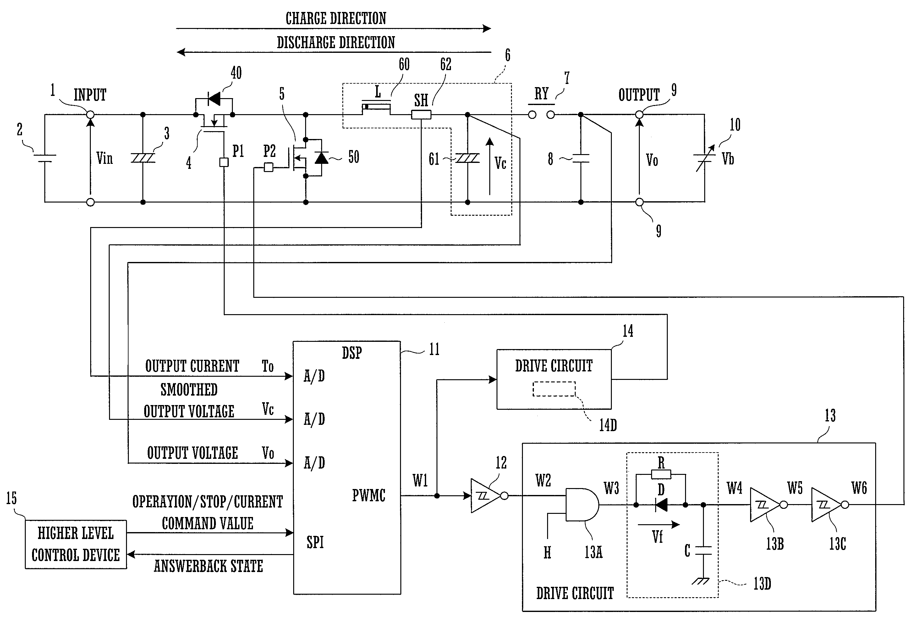
[0035]FIG. 1 is a block diagram of a charge / discharge device which is an embodiment of the present invention.

[0036]This charge / discharge device is used as a test device for testing the characteristics of a secondary battery by repeatedly charging and discharging that secondary battery.

[0037]A DC power supply unit 2 is connected to input terminals 1. Provided that its output voltage is a DC voltage, this DC power supply unit 2 may comprise a battery or an AC-DC converter or the like.

[0038]To the input terminals 1 there are connected in parallel a first smoothing capacitor 3 and a series circuit comprising a first switching element 4 and a second switching element 5. By “connected in parallel” is meant being directly or indirectly electrically connected in parallel between the input terminals 1, and includes both being connected in parallel without the interposition of any element or circuit, and being connected in parallel via some element or circuit.

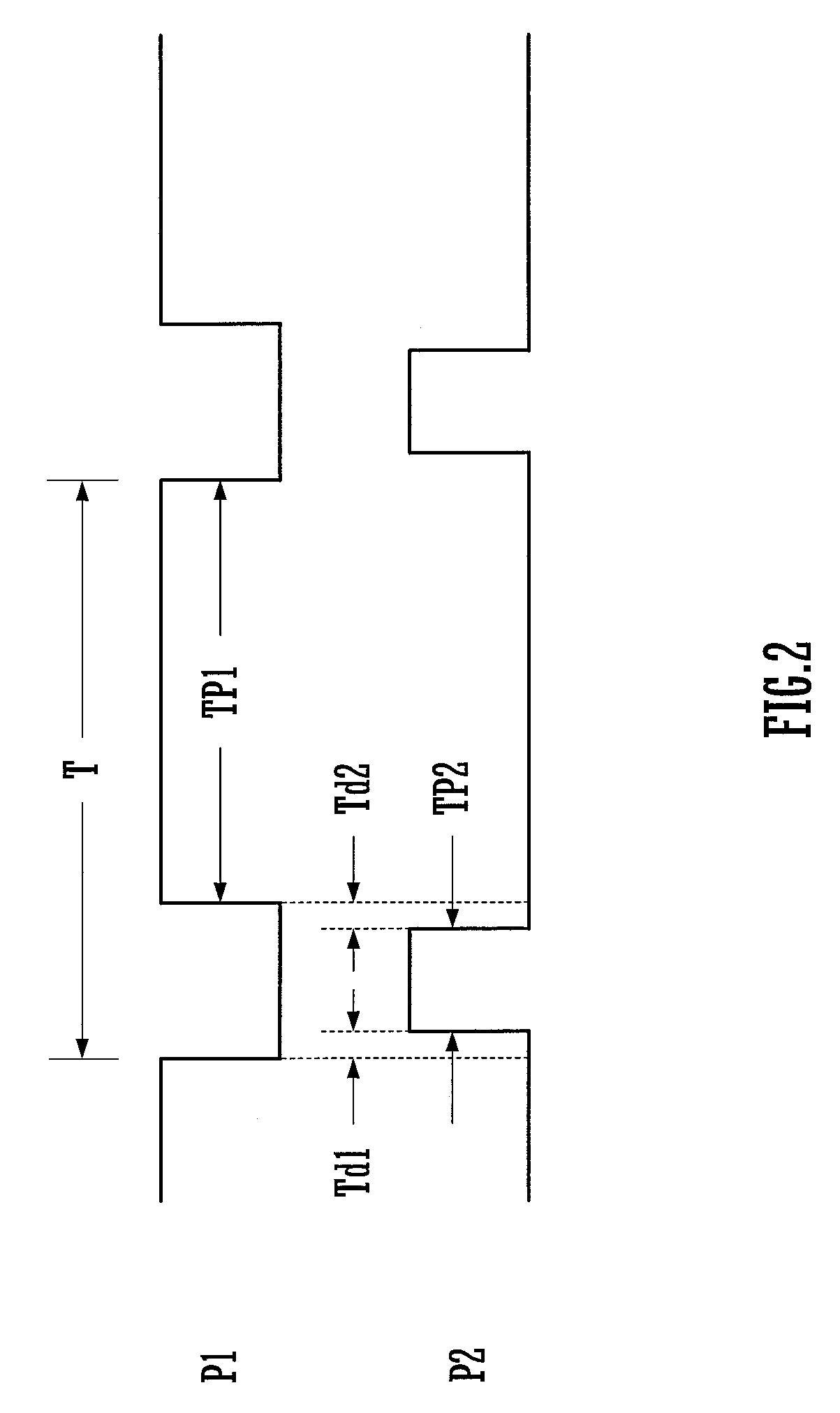
[0039]Each of the first switching...


PUM

PropertyMeasurementUnit
voltageaaaaaaaaaa
voltageaaaaaaaaaa
voltageaaaaaaaaaa

Abstract

This power supply device includes a series circuit of a first switching element and a second switching element connected in parallel with a DC power supply unit, and a smoothing filter circuit which includes a series circuit of an inductor and a smoothing capacitor connected in parallel with the second switching element. The power supply device also includes a control unit and a drive circuit for generating first and second PWM pulses by respectively driving the first and second switching elements ON and OFF, and for creating a dead time between those switching pulse signals. And this control unit changes the frequency of the switching pulse signal according to the pulse width of either the first PWM pulses or the second PWM pulses.

Description

CROSS REFERENCE[0001]This Nonprovisional application claims priority under 35 U.S.C. §119(a) on Patent Application No. 2008-070591 filed in Japan on Mar. 19, 2008, the entire contents of which are hereby incorporated by reference.BACKGROUND OF THE INVENTION[0002]The present invention relates to a charge / discharge device, and to a power supply device for a charge / discharge device or the like. In particular, it relates to a power supply device, to the output terminals of which a secondary battery is connected, and which is adapted for performing testing of the battery characteristics (the electrical discharge characteristic and the capacity and so on) of this secondary battery by repeatedly performing charge and discharge thereof.[0003]In the testing of a secondary battery such as a lithium ion battery or the like, normally, testing is performed by repeatedly charging and discharging the secondary battery by connecting it as a test subject to output terminals. For example control may ...

Claims


Application Information

Patent Timeline
Patent Type & Authority Patents(United States)
IPC IPC(8): H02J7/04H02J7/16H02J7/00G01N27/42G01N27/416H02M3/155
CPCH02M3/1582H02M1/08
Inventor YORINOBU, MASANORIOKAMOTO, SHIGERUKATSUSHIMA, HAJIME
Owner SANSHA ELECTRIC MFG
Why Eureka
Try Eureka