Circuit board connector

a technology of circuit board and connector, applied in the direction of coupling device connection, coupling protective earth/shielding arrangement, securing/insulating coupling contact member, etc., can solve problems such as signal delay (skew) and achieve the effect of preventing signal crosstalk and preventing signal delay (skew)

Inactive Publication Date: 2011-12-27
AUTONETWORKS TECH LTD +2
View PDF23 Cites 7 Cited by
  • Summary
  • Abstract
  • Description
  • Claims
  • Application Information

AI Technical Summary

Benefits of technology

[0012]In the circuit board connector according to the present invention in which the vertical portions of the terminals in the upper layer are located on the backside in the depth direction with respect to the vertical portions of the terminals in the lower layer, the upper terminals and the lower terminals do not intersect. Accordingly, a crosstalk of signals can be prevented. In addition, because the path length of the upper terminals and the path length of the lower terminals are made equal by bending, occurrence of a delay (skew) of signals is prevented without making the circuit board connector large in the depth direction.
[0013]By arranging the plurality of terminals substantially parallel to each other when viewed from the width direction, the circuit board connector is made smaller in the depth direction.
[0014]By receiving the tip portions of the bent vertical portions by the receiving grooves receiving the base portions of the vertical portions of the adjacent terminals, the receiving grooves are shared, which makes the connector smaller also in the width direction.

Problems solved by technology

When a circuit board connector is provided with a plurality of terminals, the plurality of terminals are often arranged in a plurality of layers in a height direction because of space limitations and other reasons.
Thus, in a differential manner in which data is transmitted through a pair of signal lines, a phase difference occurs between the upper terminal and the lower terminal, which could cause a delay (skew) of signals.

Method used


Image

  • Circuit board connector
  • Circuit board connector
  • Circuit board connector

Examples


Embodiment Construction

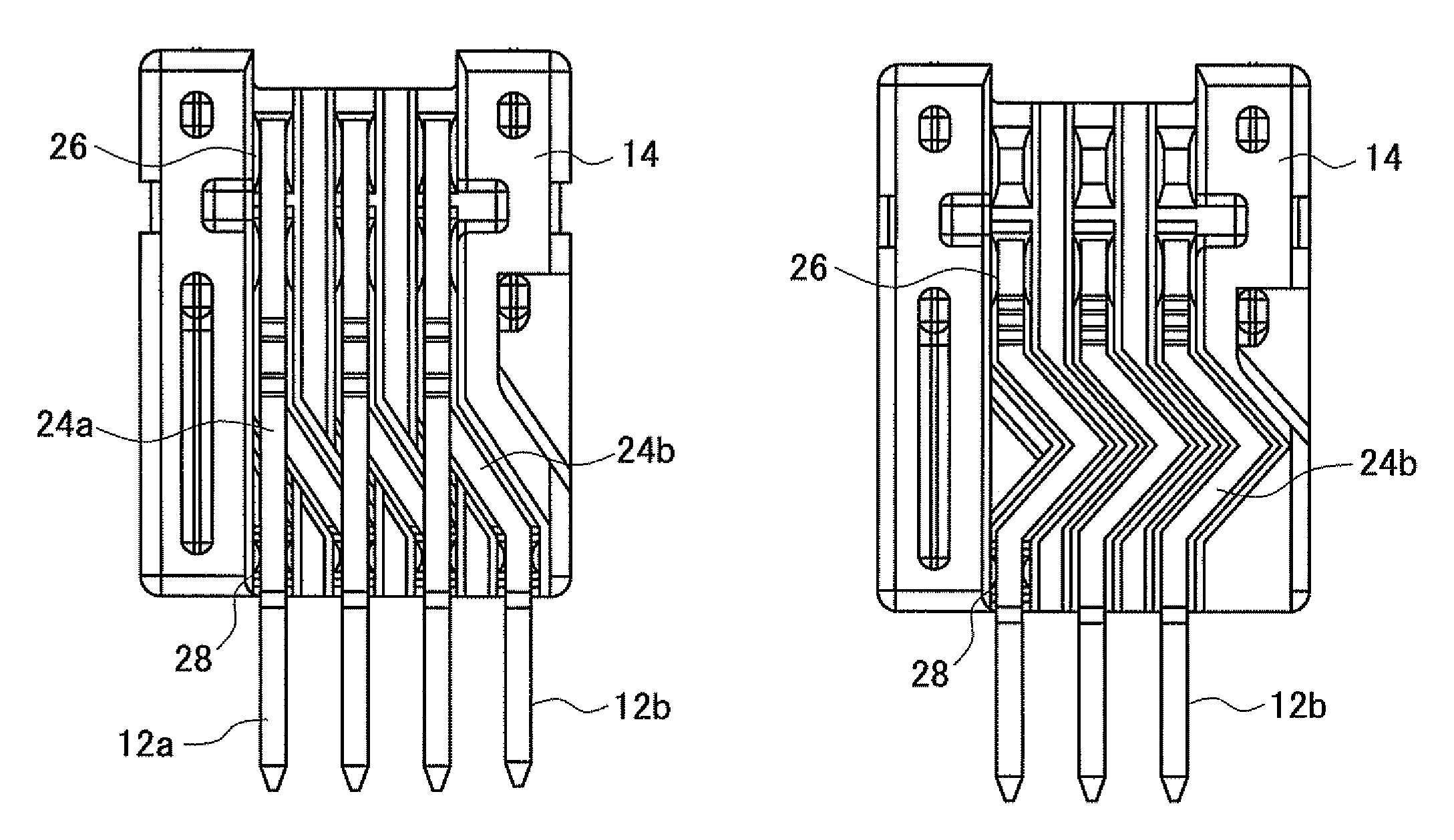
[0025]A detailed description of preferred embodiments of the present invention will now be provided with reference to the accompanying drawings. In a circuit board connector according to a preferred embodiment of the present invention, the side of the circuit board connector to be connected to an end of an electric wire is referred to as the front side, and the opposite side is referred to as the back side (the back side in the depth direction). An upper direction of a printed circuit board onto which the circuit board connector is attached is referred to as a height direction, and a direction that is perpendicular to both of the height direction and the depth direction is referred to as a width direction of the circuit board connector.

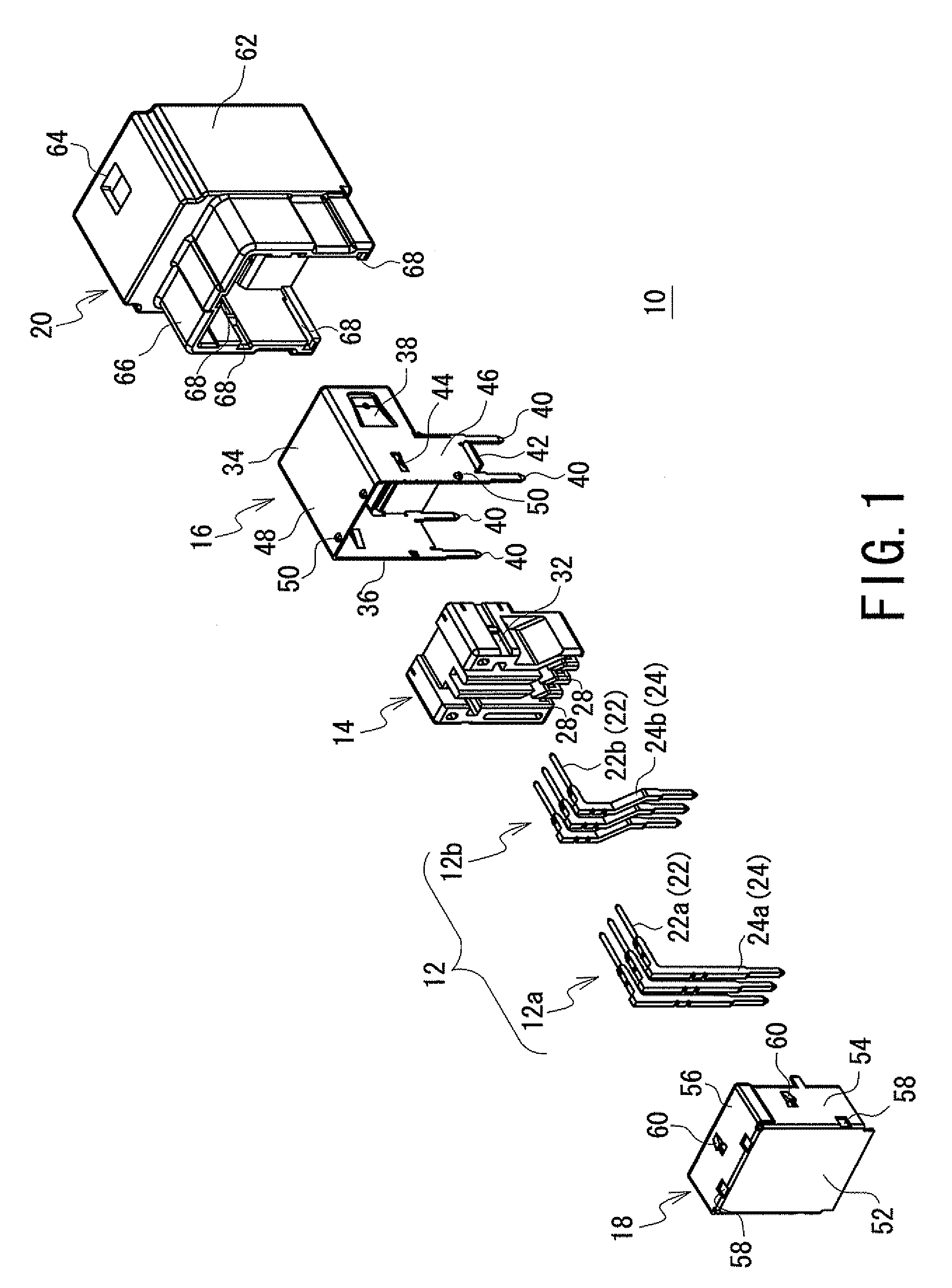
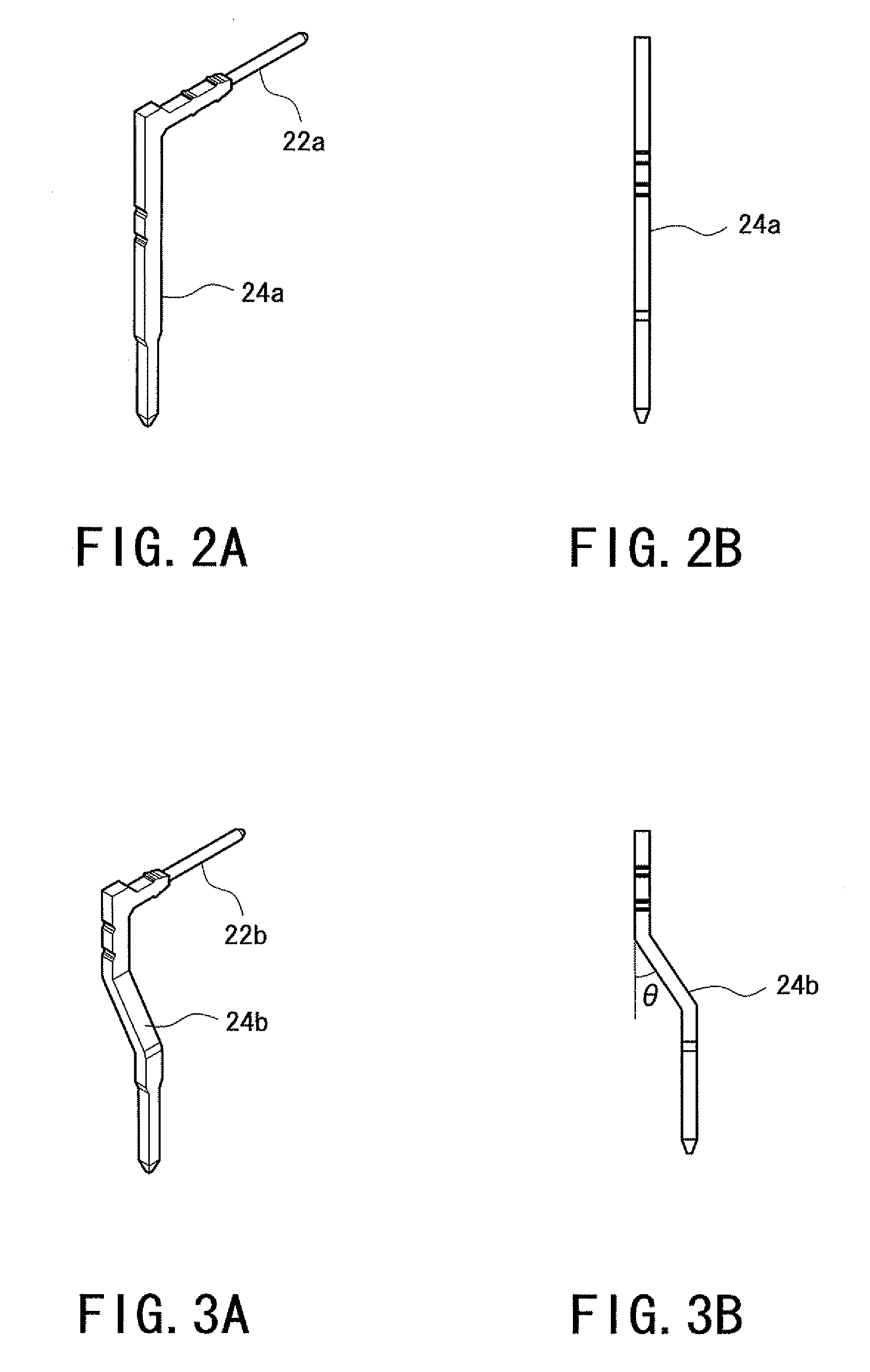
[0026]As shown in FIG. 1, a circuit board connector 10 according to a preferred embodiment of the present invention is configured such that a plurality of terminals 12 arranged to electrically connect ends of electric wires and printed wiring of a pri...


PUM


Abstract

A circuit board connector with no delay (skew) of signals and no crosstalk of signals. In a circuit board connector, a plurality of terminals having horizontal portions to be connected to ends of electric wires and vertical portions extending downward from one ends of the horizontal portions and arranged to be connected to a signal pattern of a printed circuit board are included, vertical portions of upper terminals are located on the back side of vertical portions of lower terminals, are bent in the width directions, and the path lengths of the upper terminals and of the lower terminals are equal. A tip portion of the lower terminal is received by a receiving groove of an inner housing housing a base portion of the vertical portion of the adjacent terminal.

Description

TECHNICAL FIELD[0001]The present invention relates to a circuit board connector, and specifically relates to a circuit board connector to be attached to a printed circuit board on which printed wiring is provided in order to send and receive signals to and from the printed circuit board and supply electric power to the printed circuit board.BACKGROUND ART[0002]Conventionally, an electrical / electronic appliance to be installed on a car such as an automobile is provided with a number of printed circuit boards on which electronic components, ICs (integrated circuits), and other components are mounted. To the printed circuit boards, electric wires arranged to send and receive signals to and from other devices and other printed circuit boards and supply electric power to the printed circuit boards are connected. In order to make a transit connection between the electric wires and the printed circuit boards, circuit board connectors are used.[0003]A circuit board connector is generally co...

Claims


Application Information

Patent Timeline
Patent Type & Authority Patents(United States)
IPC IPC(8): H01R12/00
CPCH01R13/658H01R13/6461H01R13/6474H01R13/6594H01R13/41H01R12/727
Inventor KOBAYASHI, KAZUMASA
Owner AUTONETWORKS TECH LTD
Why Eureka
Try Eureka