Manufacturing method of semiconductor device for enhancing the current drive capability
a manufacturing method and technology of semiconductor devices, applied in the direction of semiconductor devices, basic electric elements, electrical equipment, etc., can solve the problems of oxidation of metal films, degradation of characteristics of mos transistors, and conventional semiconductor devices, so as to reduce the thickness of silicon oxide films, and reduce the amount of hydrogen atoms
- Summary
- Abstract
- Description
- Claims
- Application Information
AI Technical Summary
Benefits of technology
Problems solved by technology
Method used
Image
Examples
first embodiment
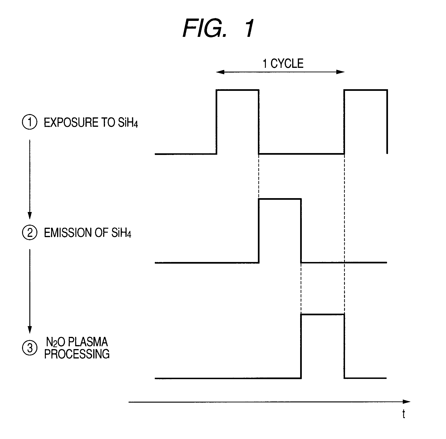
[0057]The following will describe a manufacturing method for forming a silicon oxide (SiO) film under low temperature using a commonly-used parallel-plate type plasma CVD device. As shown in FIG. 1, a silicon oxide film is formed by repeating one cycle comprised of three steps a predetermined number of times. First, in step 1, a semiconductor substrate is exposed to silane (SiH4). Then, in step 2, the remaining silane (SiH4) is emitted. Thereafter, the semiconductor substrate is exposed to nitrous oxide plasma in step 3.
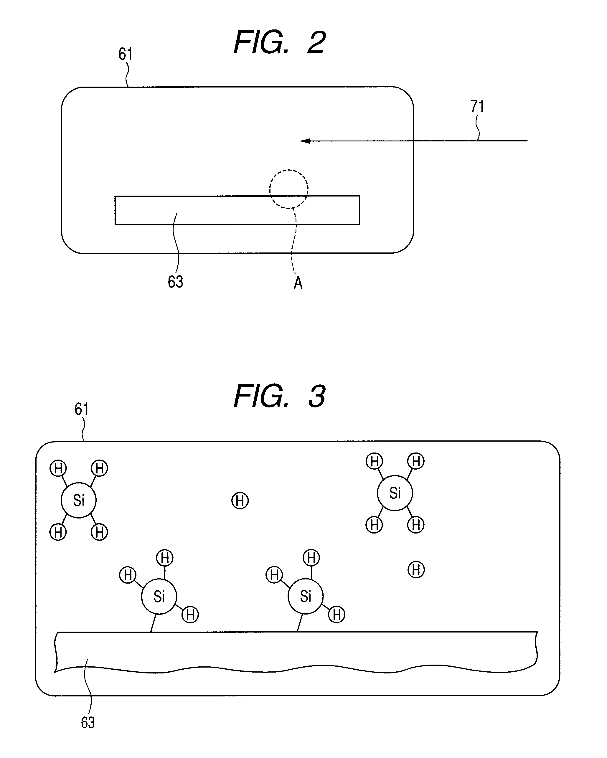
[0058]The respective steps will be descried in more detail. As shown in FIG. 2, first, a semiconductor substrate 63 is carried into a chamber 61 of the plasma CVD device. In step 1, the temperature of a heater (not shown) provided in the chamber 61 is set to about 200° C. Monosilane (SiH4) diluted with nitrous oxide (N2O) and helium (He) is introduced into the chamber 61 as a carrier gas (as indicated by the arrow 71), so that the semiconductor substrate 63 is expose...
second embodiment
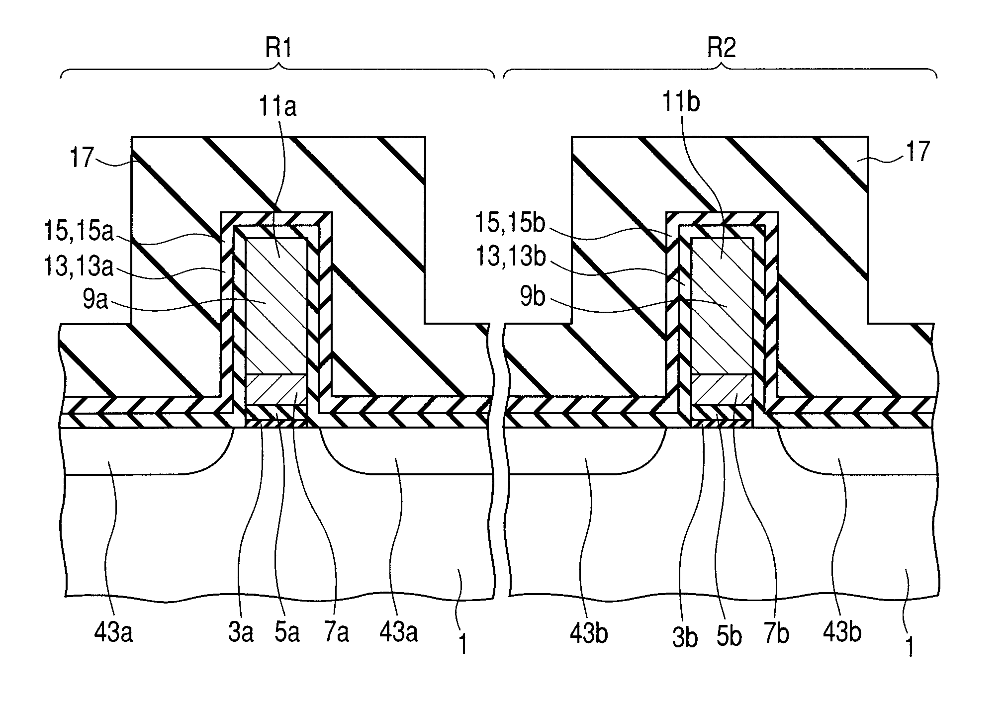
[0071]The following will describe a case where the above-mentioned forming method of the silicon oxide film (SiO film) is applied to the formation of the offset spacer of the MOS transistor.
[0072]First, as show in FIG. 10, in an nMOS region R1 of the semiconductor substrate 1, a High-k film 5a having a predetermined dielectric constant, a metal film 7a having a predetermined work function, and a polysilicon film 9a are laminated on an interlayer 3a thereby to form a gate electrode 11a of an n-channel MOSFET transistor. In contrast, in a pMOS region R2 of the semiconductor substrate 1, a High-k film 5b having a predetermined dielectric constant, a metal film 7b having a predetermined work function, and a polysilicon film 9b are laminated on an interlayer 3b thereby to form a gate electrode 11b of a p-channel MOSFET transistor.
[0073]For example, a film made of SiO, SiON, or the like is used as the interlayer 3a or 3b. For example, a hafnium-based High-k film made of HfSiON, HfON, HfO2...
third embodiment
[0099]The following will describe a manufacturing method for forming a silicon oxide (SiCO) film to which carbon is added under low temperature using the general parallel-plate type plasma CVD device. As shown in FIG. 26, the silicon oxide film with carbon added is formed by repeating one cycle including three steps a predetermined number of times. First, in step 1, a semiconductor substrate is exposed to trimethylsilane (Si(CH3)3H, hereinafter referred to as “TMS”). Then, in step 2, the remaining trimethylsilane (TMS) is emitted or exhausted. And in step 3, the semiconductor substrate is exposed to nitrous oxide plasma.
[0100]Each step will be described below in more detail. As shown in FIG. 27, first, the semiconductor substrate 63 is carried into the chamber 61 of the plasma CVD device. In step 1, the temperature of the heater provided in the chamber 61 is set to about 200° C. Trimethylsilane (TMS) diluted with nitrous oxide (N2O) and helium (He) is introduced into the chamber 61 ...
PUM
| Property | Measurement | Unit |
|---|---|---|
| thickness | aaaaa | aaaaa |
| temperature | aaaaa | aaaaa |
| thickness | aaaaa | aaaaa |
Abstract
Description
Claims
Application Information


