Manufacturing method of semiconductor device

a manufacturing method and semiconductor technology, applied in the direction of semiconductor devices, basic electric elements, electrical equipment, etc., can solve the problems of oxidation of metal films, degradation of characteristics of mos transistors, and conventional semiconductor devices, so as to reduce the thickness of silicon oxide films, and reduce the amount of hydrogen atoms

Inactive Publication Date: 2011-01-06
RENESAS ELECTRONICS CORP
View PDF4 Cites 66 Cited by
  • Summary
  • Abstract
  • Description
  • Claims
  • Application Information

AI Technical Summary

Benefits of technology

[0011]The present invention has been proposed as part of the above development, and it is an object of the present invention to provide a manufacturing method of a semiconductor device which can uniformly form a good and thin silicon oxide film or the like as an offset spacer at a relatively low temperature.
[0014]In the manufacturing method of a semiconductor device according to the invention, the silicon oxide film serving as the offset spacer can be formed under a temperature condition of about 200° C., which can prevent the oxidization of the metal film of the gate electrode. Further, the good silicon oxide film can be formed in which the amount of hydrogen atoms is reduced. Moreover, the thickness of the silicon oxide film can be accurately controlled by changing the number of cycles in the manufacturing method.
[0015]In the manufacturing method of a semiconductor device according to the invention, the silicon oxide film containing added carbon and serving as the offset spacer can be formed under a temperature condition of about 200° C., which can prevent the oxidization of the metal film of the gate electrode. Further, the good silicon oxide film with carbon added can be formed in which the amount of hydrogen atoms is reduced. Moreover, the thickness of the silicon oxide film can be accurately controlled by changing the number of cycles in the manufacturing method.

Problems solved by technology

The conventional semiconductor devices, however, have the following problems.
When a silicon oxide film is intended to be formed by a decompression chemical vapor deposition (CVD) method as an offset spacer for a gate electrode formed using a High-k film and a metal film, the temperature of deposition is relatively high to possibly cause the oxidization of the metal film.
This leads to degradation in characteristics of a MOS transistor, such as variations in resistance or the like thereof.
In contrast, when a silicon oxide film is intended to be formed at a relatively low temperature, a fragile silicon oxide film is generally formed, which makes it difficult to form a good silicon oxide film.
For example, a high hydrogen content of the silicon oxide film causes failures, including negative bias temperature instability (NBTI), especially in the p-channel type MOSFET (MOS Field Effective Transistor).

Method used


Image

  • Manufacturing method of semiconductor device
  • Manufacturing method of semiconductor device
  • Manufacturing method of semiconductor device

Examples


first embodiment

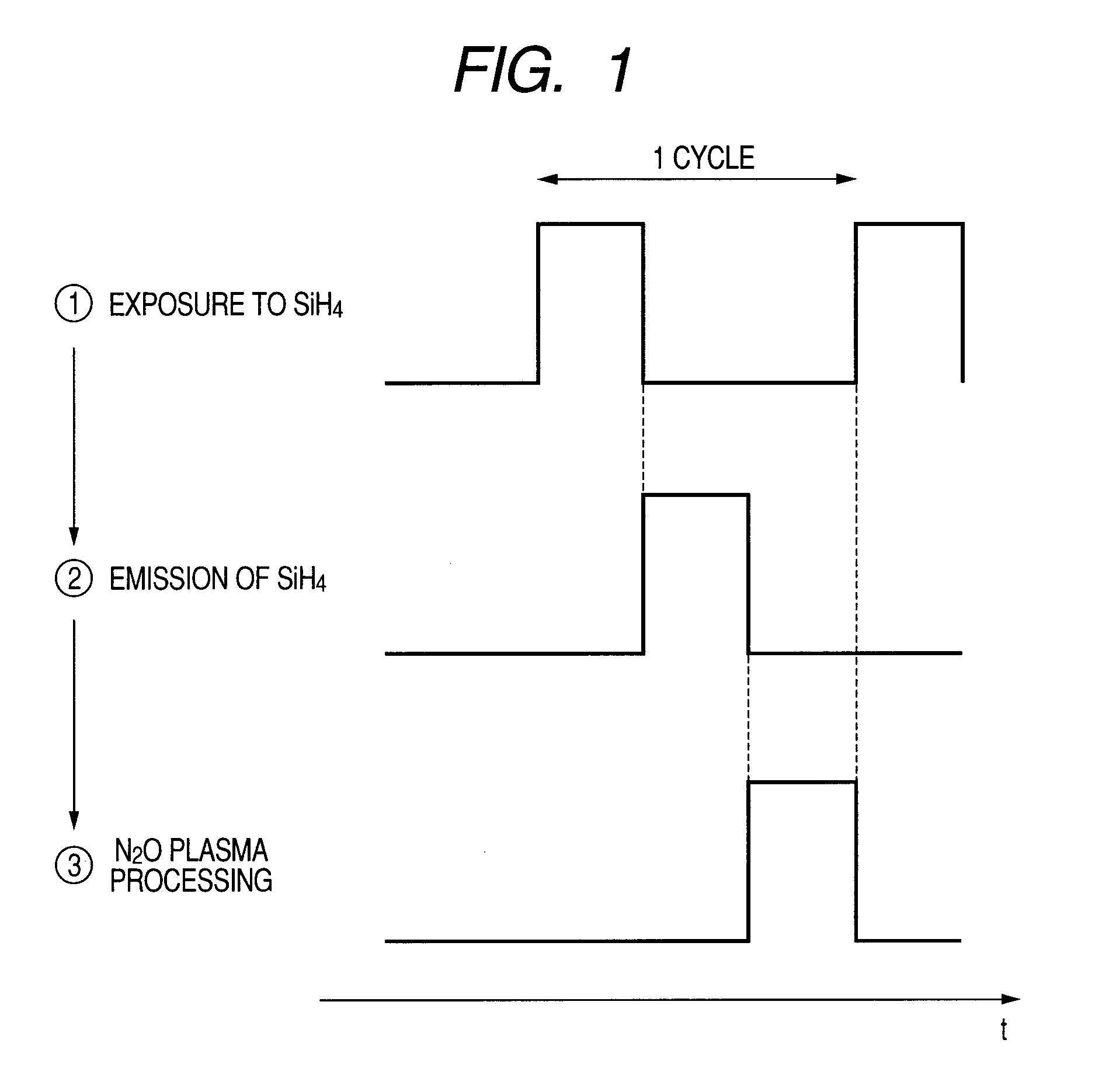
[0057]The following will describe a manufacturing method for forming a silicon oxide (SiO) film under low temperature using a commonly-used parallel-plate type plasma CVD device. As shown in FIG. 1, a silicon oxide film is formed by repeating one cycle comprised of three steps a predetermined number of times. First, in step 1, a semiconductor substrate is exposed to silane (SiH4) Then, in step 2, the remaining silane (SiH4) is emitted. Thereafter, the semiconductor substrate is exposed to nitrous oxide plasma in step 3.

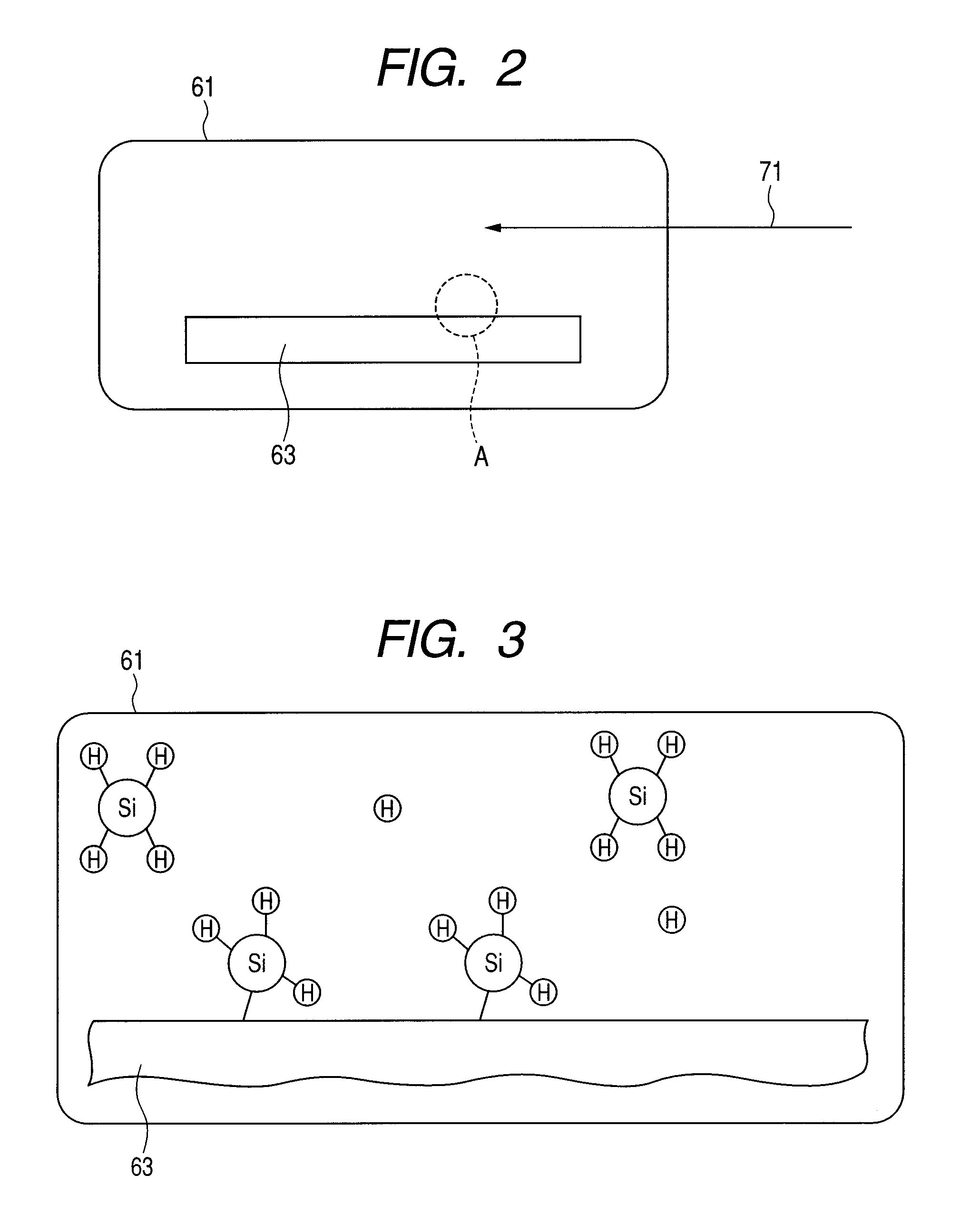
[0058]The respective steps will be descried in more detail. As shown in FIG. 2, first, a semiconductor substrate 63 is carried into a chamber 61 of the plasma CVD device. In step 1, the temperature of a heater (not shown) provided in the chamber 61 is set to about 200° C. Monosilane (SiH4) diluted with nitrous oxide (N2O) and helium (He) is introduced into the chamber 61 as a carrier gas (as indicated by the arrow 71), so that the semiconductor substrate 63 is exposed...

second embodiment

[0071]The following will describe a case where the above-mentioned forming method of the silicon oxide film (SiO film) is applied to the formation of the offset spacer of the MOS transistor.

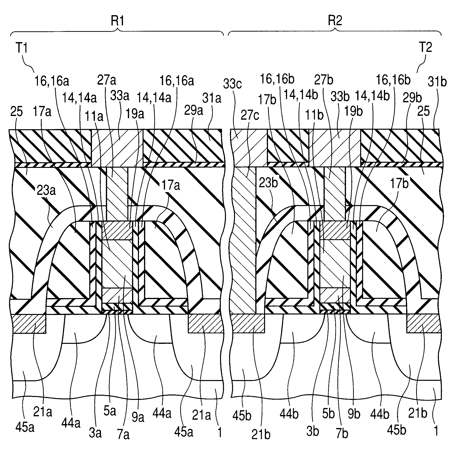
[0072]First, as show in FIG. 10, in an nMOS region R1 of the semiconductor substrate 1, a High-k film 5a having a predetermined dielectric constant, a metal film 7a having a predetermined work function, and a polysilicon film 9a are laminated on an interlayer 3a thereby to form a gate electrode 11a of an n-channel MOSFET transistor. In contrast, in a pMOS region R2 of the semiconductor substrate 1, a High-k film 5b having a predetermined dielectric constant, a metal film 7b having a predetermined work function, and a polysilicon film 9b are laminated on an interlayer 3b thereby to form a gate electrode 11b of a p-channel MOSFET transistor.

[0073]For example, a film made of SiO, SiON, or the like is used as the interlayer 3a or 3b. For example, a hafnium-based High-k film made of HfSiON, HfON, HfO2...

third embodiment

[0099]The following will describe a manufacturing method for forming a silicon oxide (SiCO) film to which carbon is added under low temperature using the general parallel-plate type plasma CVD device. As shown in FIG. 26, the silicon oxide film with carbon added is formed by repeating one cycle including three steps a predetermined number of times. First, in step 1, a semiconductor substrate is exposed to trimethylsilane (Si(CH3)3H, hereinafter referred to as “TMS”). Then, in step 2, the remaining trimethylsilane (TMS) is emitted or exhausted. And in step 3, the semiconductor substrate is exposed to nitrous oxide plasma.

[0100]Each step will be described below in more detail. As shown in FIG. 27, first, the semiconductor substrate 63 is carried into the chamber 61 of the plasma CVD device. In step 1, the temperature of the heater provided in the chamber 61 is set to about 200° C. Trimethylsilane (TMS) diluted with nitrous oxide (N2O) and helium (He) is introduced into the chamber 61 ...


PUM

PropertyMeasurementUnit
thicknessaaaaaaaaaa
temperatureaaaaaaaaaa
thicknessaaaaaaaaaa

Abstract

A manufacturing method of a semiconductor device is provided which can uniformly form a good and thin silicon oxide film or the like at a relatively low temperature. In step 1, a semiconductor substrate is exposed to monosilane (SiH4). Then, in step 2, the remaining monosilane (SiH4) is emitted. In step 3, the semiconductor substrate is exposed to nitrous oxide plasma. A desired silicon oxide film is formed by repeating one cycle including steps 1 to 3 until a necessary thickness of the film is obtained.

Description

CROSS-REFERENCE TO RELATED APPLICATIONS[0001]The disclosure of Japanese Patent Application No. 2009-158888 filed on Jul. 3, 2009 including the specification, drawings and abstract is incorporated herein by reference in its entirety.BACKGROUND OF THE INVENTION[0002]The present invention relates to manufacturing methods of semiconductor devices, and more particularly, to a manufacturing method of a semiconductor device including a metal oxide semiconductor (MOS) transistor.[0003]In recent years, metal oxide semiconductor (MOS) transistors have been required to have an improved current drive capability so as to achieve higher performance of an electronic device and reduction in consumed power of the device. In order to enhance the current drive capability, gate electrodes have been developed which include an insulating film having a higher dielectric constant (High-k film) than that of a SiO2 film or a SiON film as a gate insulating film, and a metal film made of metal material having ...

Claims


Application Information

Patent Timeline
Patent Type & Authority Applications(United States)
IPC IPC(8): H01L21/8238
CPCH01L21/02126H01L21/02164H01L21/02211H01L21/02274H01L21/0228H01L21/28247H01L2924/0002H01L21/823807H01L21/823864H01L29/7843H01L2924/00
Inventor MURATA, TATSUNORIMIYAGAWA, YOSHIHIRO
Owner RENESAS ELECTRONICS CORP
Why Eureka
Try Eureka