Supercharge Your Innovation With Domain-Expert AI Agents!

Array substrate receiving two polarities opposite to each other and a display device having the same

a display device and array substrate technology, applied in static indicating devices, instruments, optics, etc., can solve the problems of increasing power consumption of lcd devices, gradual deterioration of liquid crystal layers, etc., and achieve the effect of preventing the reduction of the aperture ratio of the display devi

Active Publication Date: 2011-12-27
SAMSUNG DISPLAY CO LTD
View PDF16 Cites 4 Cited by
  • Summary
  • Abstract
  • Description
  • Claims
  • Application Information

AI Technical Summary

Benefits of technology

[0013]Embodiments of the present invention provide an array substrate capable of reducing power consumption and increasing an aperture ratio thereof in order to enhance a luminance of a display device and a display device having the above-mentioned array substrate.
[0017]According to the array substrate and the display device described above, a polarity of a data signal that is applied to the pixel elements is controlled by a gate signal that is applied to each of plurality of gate lines, so that the driven display device consumes a relatively small amount of power and a decrease in aperture ratio of the display device is prevented.

Problems solved by technology

When a voltage having a predetermined polarity is continuously applied to a first electrode and a second electrode that are adjacent to a liquid crystal of an LCD device, the liquid crystal layer is gradually deteriorated.
When the inversion frequency of the common voltage increases, however, the power consumption of the LCD device also increases.

Method used


Image

  • Array substrate receiving two polarities opposite to each other and a display device having the same
  • Array substrate receiving two polarities opposite to each other and a display device having the same
  • Array substrate receiving two polarities opposite to each other and a display device having the same

Examples


Embodiment Construction

[0026]Exemplary embodiments of the present invention are described more fully hereinafter with reference to the accompanying drawings. This invention may, however, be embodied in many different forms and should not be construed as limited to the embodiments set forth herein.

[0027]Hereinafter, the present invention will be described in detail with reference to the accompanying drawings.

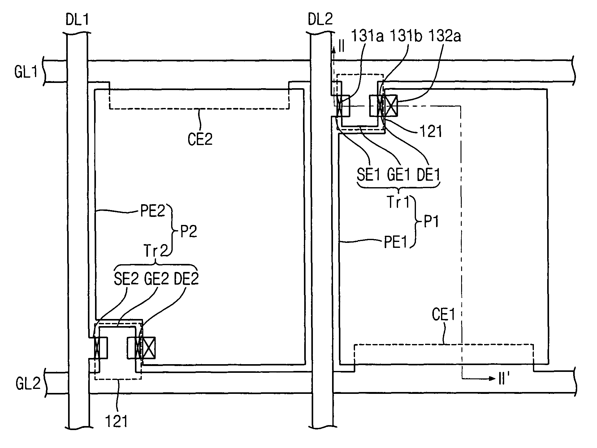
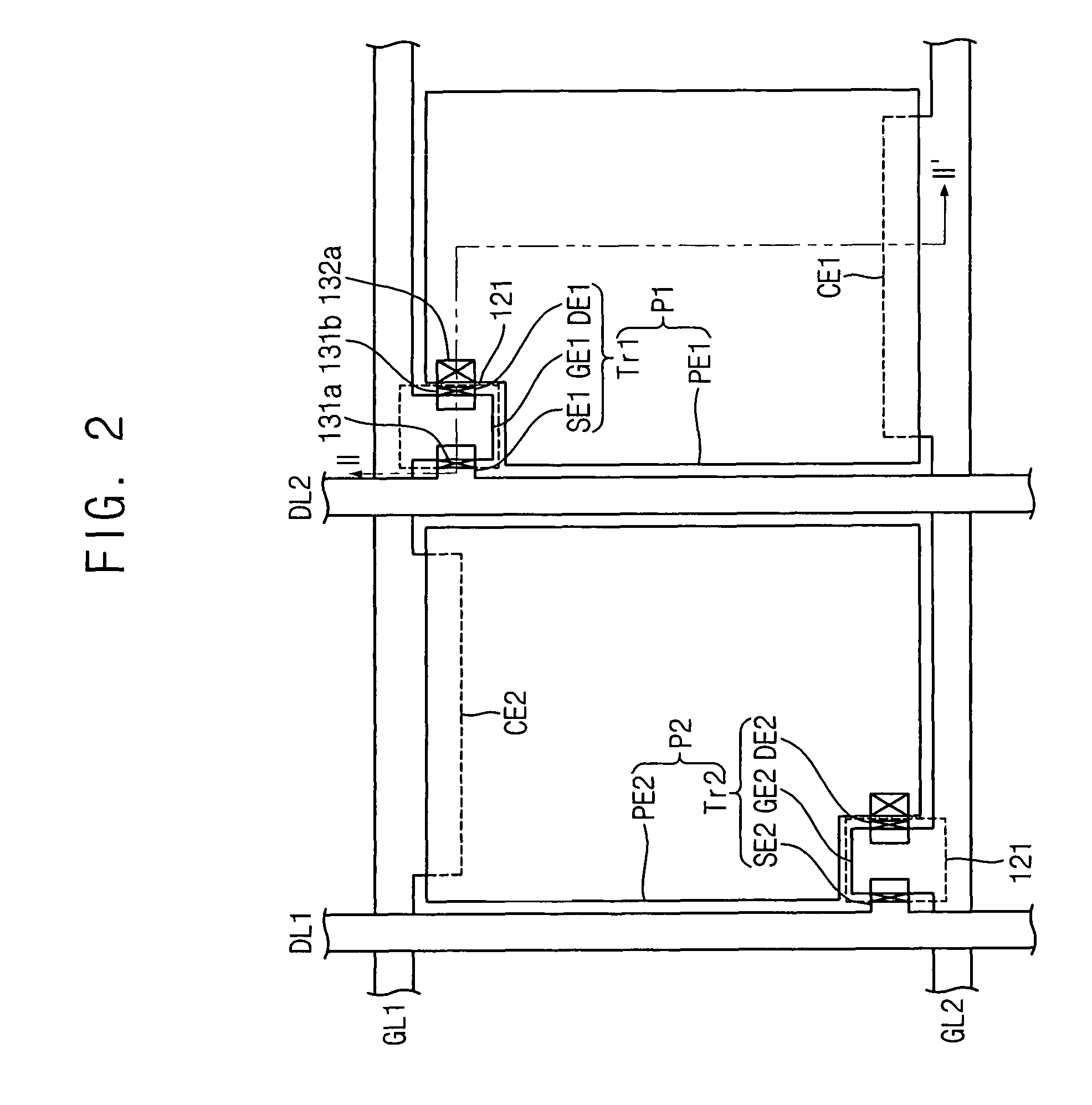
[0028]FIG. 1 is an equivalent schematic circuit diagram illustrating an array substrate according to an exemplary embodiment of present invention.

[0029]Referring to FIG. 1, an array substrate 100 includes a plurality of gate lines GL1˜GLn+1 and a plurality of data lines DL1˜DLm. The gate lines GL1˜GLn+1 and the data lines DL1˜DLm define a plurality of pixel areas arranged in a matrix shape, wherein ‘n’ and ‘m’ are natural numbers. The array substrate 100 includes a pixel array. The pixel array includes (n×m)-number of pixel elements that are defined by the n gate lines and the m data lines. In summary,...


PUM


Abstract

An array substrate includes a base substrate, a plurality of gate lines, a plurality of data lines and a pixel matrix. The plurality of gate lines and the plurality of data lines define pixel areas. The pixel matrix is formed on each pixel area, and includes a plurality of pixel columns and pixel rows. Each pixel column has a first pixel group and a second pixel group. The first pixel group is electrically connected to a first gate line adjacent to the pixel column. The second pixel group is electrically connected to a second gate line adjacent to the pixel column. Each pixel row is electrically connected to one data line adjacent to the pixel column.

Description

CROSS-REFERENCE TO RELATED APPLICATIONS[0001]This application relies for priority upon Korean Patent Application No. 2005-62476 filed on Jul. 12, 2005, the contents of which are herein incorporated by reference in its entirety.BACKGROUND OF THE INVENTION[0002]1. Technical Field[0003]The present disclosure relates to an array substrate and a display device having the array substrate. More particularly, the present disclosure relates to an array substrate capable of reducing power consumption and enhancing an image display quality and a display device having the array substrate.[0004]2. Discussion of the Related Art[0005]Generally, a liquid crystal display (LCD) device includes an array substrate, an opposite substrate that faces the array substrate and a liquid crystal layer disposed between the array substrate and the opposite substrate.[0006]The array substrate includes a plurality of data lines extended along a first direction, a plurality of gate lines extended along a second dir...

Claims


Application Information

Patent Timeline
Patent Type & Authority Patents(United States)
IPC IPC(8): G09G3/36
CPCG02F1/134336G09G3/3614G02F1/136286G02F2201/40G09G3/3677G02F1/133
Inventor JOO, SOONG-YONGKANG, MYUNG-KOOZHANG, LINTAOLEE, JUNG-SUNJUNG, SUK-KILEE, DONG-YUBPARK, JONG-HWA
Owner SAMSUNG DISPLAY CO LTD
Features
  • R&D
  • Intellectual Property
  • Life Sciences
  • Materials
  • Tech Scout
  • Unparalleled Data Quality
  • Higher Quality Content
  • 60% Fewer Hallucinations
Learn More