Methods for mounting an electro-optical component in alignment with an optical element and related structures

a technology of electrooptical components and optical elements, applied in the direction of optics, instruments, optical light guides, etc., can solve the problems of insufficient accuracy of alignment, add to final positioning uncertainty, and come at a price, and achieve satisfactory electrical connection and satisfactory electrical connection

Active Publication Date: 2011-12-27
LUMILEDS
View PDF9 Cites 1 Cited by
  • Summary
  • Abstract
  • Description
  • Claims
  • Application Information

AI Technical Summary

Benefits of technology

[0011]The present invention is based on the fact that during the soldering process of an electrical component, in particular a surface mount device (SMD) component, the component “flows” in the molten solder towards a certain well-defined end position governed by the surface tensions laws. According to the invention, the solder pads on the substrate are positioned such that the electro-optical component is brought into abutment with the optical element, thereby ensuring an accurate relative positioning between the electro-optical component and the optical element.
[0017]Preferably, the solder pads on the carrier substrate have such an extension that they completely support corresponding pads on the electro-optical component during the entire self-alignment process. In other words, regardless of when the self-alignment is interrupted by the abutment of the electro-optical component against the optical element, the solder pads will have complete contact, thus ensuring a satisfactory electrical connection.
[0021]The size and form of the two likely differs and which to choose to bring into abutment with the optical element depends on the application. Typically, the submount is more robust, and therefore more suitable to use as an alignment abutment.
[0023]The electro-optical component can be soldered using a reflow soldering process. Such a soldering process can be advantageous for creating self-alignment conditions.

Problems solved by technology

Though satisfactory alignment is feasible, it comes at a price, e.g. in terms of limitations regarding mounting process order.
However, this does not eliminate the problem of accurate alignment.
In this process, each step has its associated tolerances, which add up to the final positioning uncertainty.
In many cases, this uncertainty is too large.
Such accuracy is not feasible for the chain of tolerances described above.

Method used


Image

  • Methods for mounting an electro-optical component in alignment with an optical element and related structures
  • Methods for mounting an electro-optical component in alignment with an optical element and related structures
  • Methods for mounting an electro-optical component in alignment with an optical element and related structures

Examples


Embodiment Construction

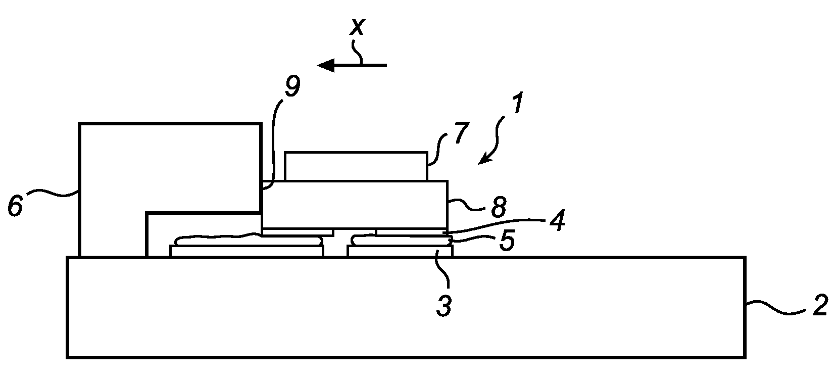
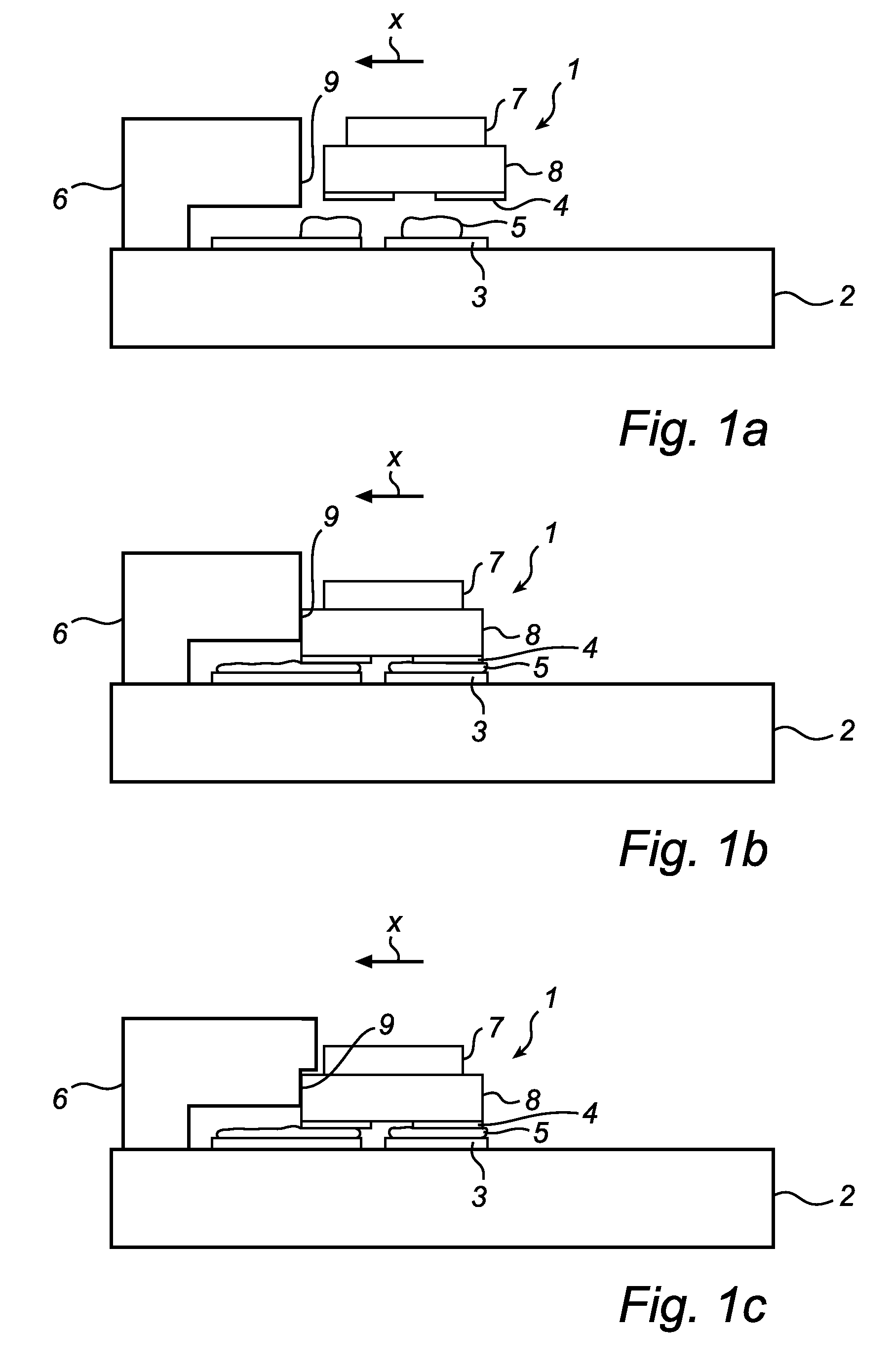
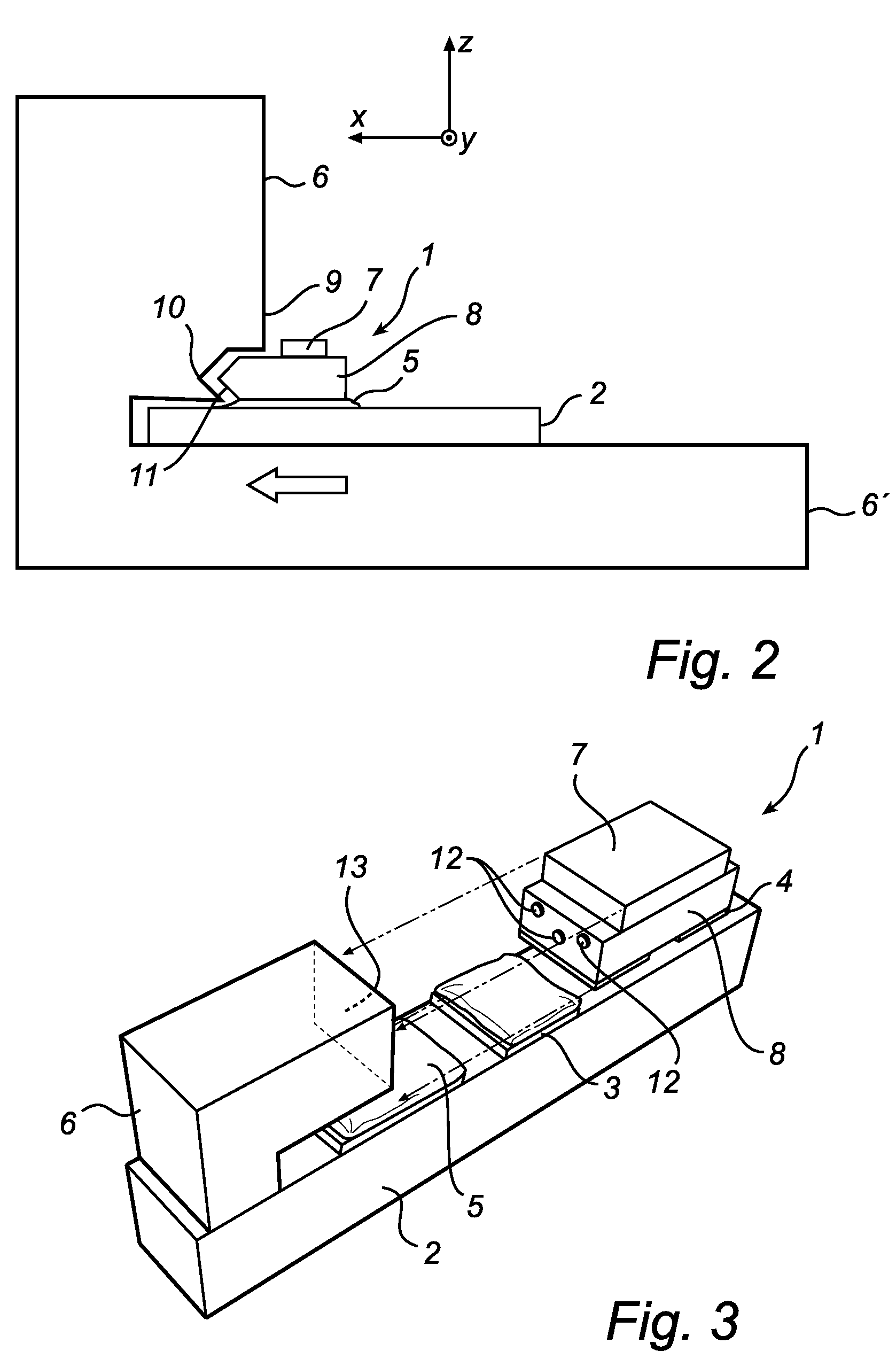
[0031]FIG. 1a-1c show a mounting structure, i.e. a collection of components, arranged for mounting an electro-optical component 1 accurately in relation to an optical element 6.

[0032]The electro-optical component 1 can be a LED or a photodiode, and typically is a “die-on-ceramics” (DoC) type component, i.e. a die mounted on a submount for subsequent mounting on a carrier substrate, such as a PCB. In FIG. 1a, the electro-optical component 1 comprises a LED die 7 on a submount 8. The electro-optical component can of course comprise more than one LED.

[0033]Reference number 2 denotes a carrier substrate, on which solder pads 3 also referred to as a “footprint”, are arranged. This footprint can serve multiple purposes, for example, but not limited to electrical connection, mechanical connections and thermal connections, and any combination thereof. Corresponding solder pads 4 are provided on the DoC 1, and solder material 5 is placed in between said solder pads 3 and 4. The solder materi...


PUM


Abstract

Mounting an electro-optical component (1) on a carrier substrate (2) in an accurate position with respect to an optical element (6), the carrier substrate and the electro-optical component each being provided with at least one solder pad (3, 4). The solder pads are arranged such that, when said electro-optical component is soldered onto the pads, a force is generated that acts on the electro-optical component in a direction (x) towards the optical element, and the structure is designed to allow said electro-optical component to move laterally during soldering, such that it is brought into abutment with said optical element, thereby ensuring an accurate relative positioning between the electro-optical component and the optical element.

Description

[0001]This application is a national stage application under 35 U.S.C. §371 of International[0002]Application No. PCT / IB2007 / 052784 filed on Jul. 12, 2007, and published in the English language on Jan. 24, 2008, as International Publication No. WO / 2008 / 010160, which claims priority to European Application No. 06117193.0, filed on Jul. 14, 2006, incorporated herein by reference.TECHNICAL FIELD OF THE INVENTION[0003]The present invention relates to a method for mounting an electro-optical component in an accurate position with respect to an optical element, comprising soldering the electro-optical component onto a carrier substrate being fixedly arranged in relation to the optical element, using soldering pads provided on the electro-optical component and the carrier substrate respectively.BACKGROUND ART[0004]In applications involving electro-optical components such as LEDs, it is sometimes important to ensure accurate alignment of these components in relation to an optical element.[0...

Claims


Application Information

Patent Timeline
Patent Type & Authority Patents(United States)
IPC IPC(8): G02B6/26H01L33/60
CPCG02B6/4232G02B6/4204
Inventor LENDERINK, EGBERTPETERS, RALPH H.SCHUG, JOSEF A.DE SAMBER, MARC A.
Owner LUMILEDS
Why Eureka
Try Eureka