Memory element and display device

a technology of memory elements and display devices, applied in semiconductor devices, digital storage, instruments, etc., can solve the problems of difficult promotion of multiple bits, reduced display desired, and inability to obtain bright pictures, etc., to achieve small area, reduce power consumption, and simplify the effect of circuit scal

Inactive Publication Date: 2012-02-14
JAPAN DISPLAY INC
View PDF15 Cites 14 Cited by
  • Summary
  • Abstract
  • Description
  • Claims
  • Application Information

AI Technical Summary

Benefits of technology

[0008]The search of the technique is emerging such that when there is no change in input video signal as in the case or the like of a still image, the data held with the memory function within each of the pixels is continued to be displayed in the form of the still image in order to reduce the number of times of the charge and discharge of the data lines, thereby promoting the low power consumption.
[0013]According to the embodiments of the present invention, the memory element is composed of the thin film transistor (TFT) and the resistance change element (ReRAM). The circuit scale is very simplified and miniaturized as compared with the existing SRAM (Static Random Access Memory). A plurality of memory elements thus miniaturized is readily incorporated in the pixel, and thus the memory having a multiple bit configuration can be built in the pixel with a small area. Therefore, it is possible to realize the active matrix type display device which is capable of performing multiple gradation display with the practical pixel size.
[0014]Since the multiple bit memory can be built in the pixel, it is possible to reduce the power consumption which is necessary for the charge and discharge for the data lines and which occupies the most part of the power consumption in the liquid crystal display panel except for a backlight. As a result, it is possible to realize the liquid crystal display panel of the active matrix type liquid crystal display device which is capable of being driven with the low power consumption. Incorporating such a liquid crystal panel in a monitor of a mobile device results in that the reduction of the battery volume as well as the prolonging of intervals of charging of a battery can be carried out. As a result, it is possible to further miniaturize the mobile device.

Problems solved by technology

In this case, it may be impossible to obtain a bright picture because the area of the pixel openings adapted to transmit a light, from a backlight, desired for the display is reduced.
As a result, when an existing memory element is tried to be directly incorporated in each of the pixels, it becomes difficult to promote the multiple bits, and thus there occurs a restriction to the high-definition and multiple gradation display.
This becomes a problem to be solved.
However, the practical level is not reached because a suitable material for the ferroelectric substance having the memory function is poor.
Thus, it is said that it is difficult to ensure the reliability of the memory function because the ferroelectric characteristics and the insulating property are easy to change when data is rewritten repeatedly.

Method used


Image

  • Memory element and display device
  • Memory element and display device
  • Memory element and display device

Examples


first embodiment

Entire Configuration

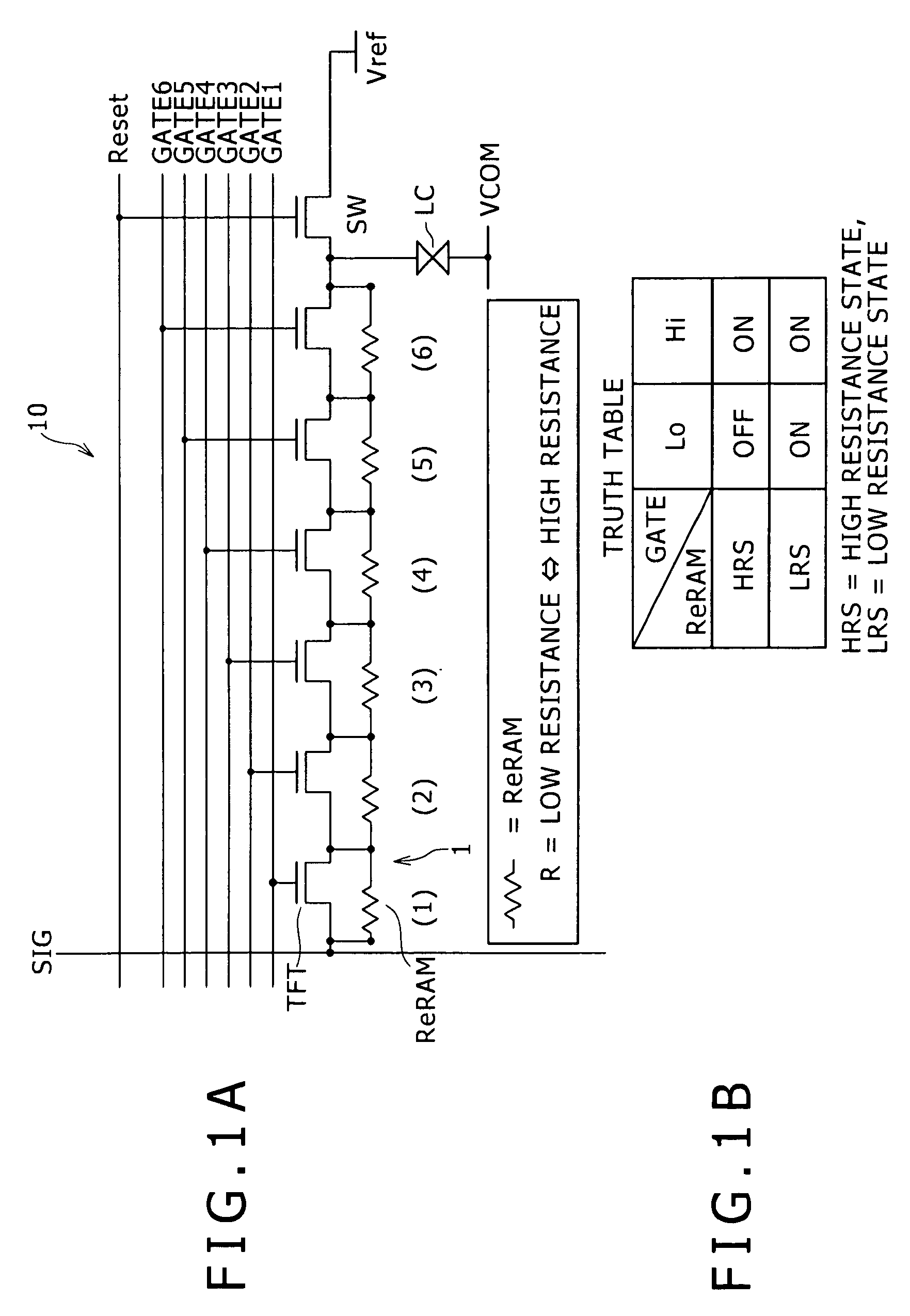
[0027]FIGS. 1A and 1B are respectively a schematic diagram showing a configuration of a memory element and a display device according to a first embodiment of the present invention, and a diagram showing a truth table. This schematic diagram is a schematic circuit diagram showing a portion for one pixel of an active matrix type liquid crystal display device. A pixel 10 includes a memory element 1.

[0028]As shown in FIG. 1A, the memory element 1 is composed of a parallel combination of a thin film transistor TFT and a resistance change element ReRAM. The TFT includes a semiconductor thin film in which a channel region, and an input terminal and an output terminal (a source and a drain) located on both sides of the channel region, respectively, are formed, and a gate electrode overlapping the channel region through an insulating film to become a control terminal. The resistance change element ReRAM is composed of one conductive layer connected to the input terminal ...

example 1

STRUCTURAL EXAMPLE 1 OF RESISTANCE CHANGE ELEMENT

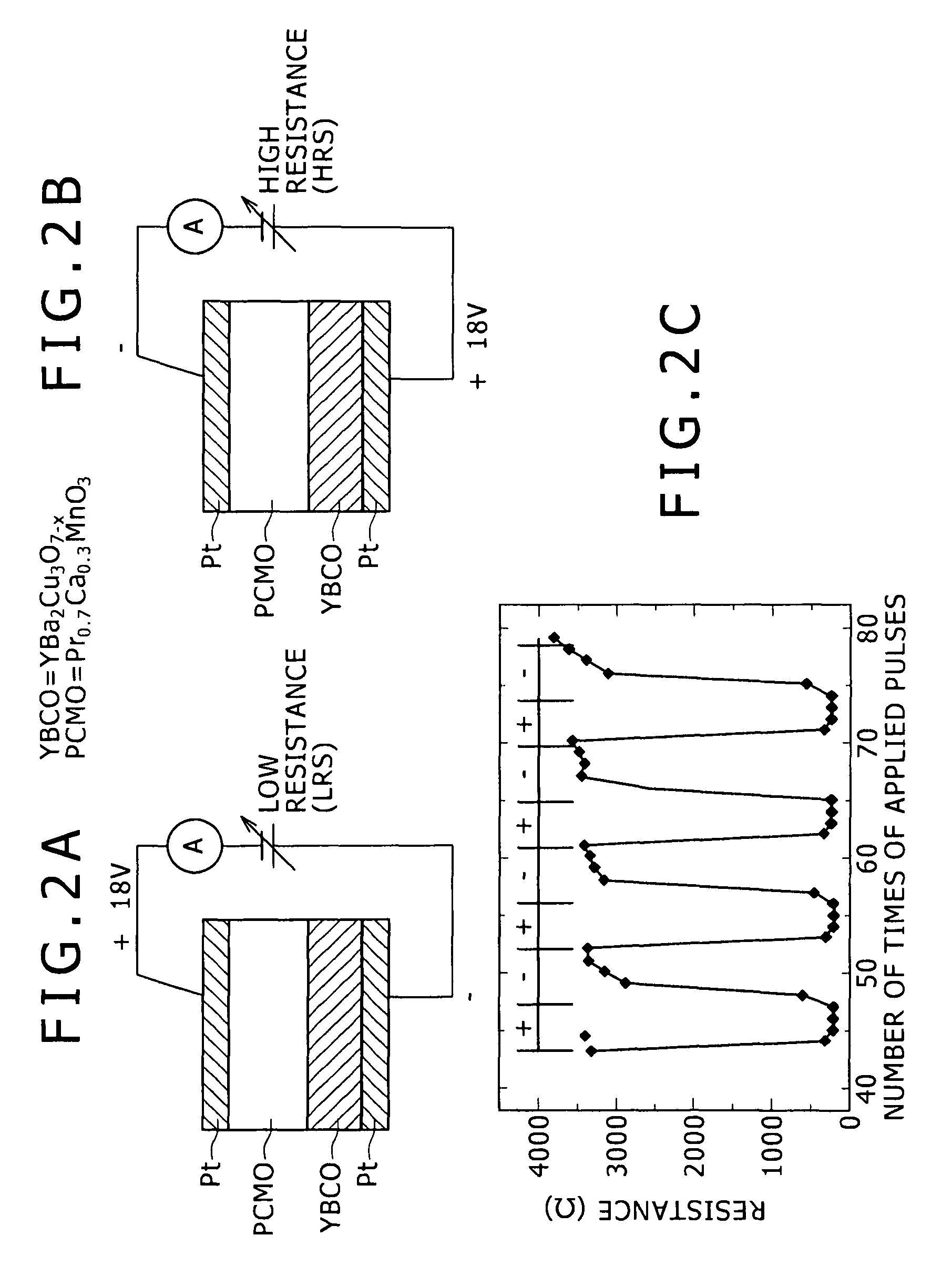
[0039]FIGS. 2A and 2B are respectively schematic views showing a concrete structural example of the resistance change element ReRAM. Here, FIG. 2A shows the low resistance state LRS of the resistance change element ReRAM, and FIG. 2B shows the high resistance state HRS of the resistance change element ReRAM. As shown in these figures, the resistance change element ReRAM is composed of a pair of conductive layers, and at least one oxide layer disposed between the conductive layers paired with each other. In the structural example shown in these figures, each of the paired conductive layers is made of a metal Pt (platinum), and two layers of metallic oxide films made of PCMO and YBCO, respectively, are formed between the paired conductive layers. That is to say, in this structural example, the oxide layers are made of the metallic oxides, respectively. When the voltage having the positive polarity of, for example, +18 V is applied to th...

second embodiment

Manufacturing Processes

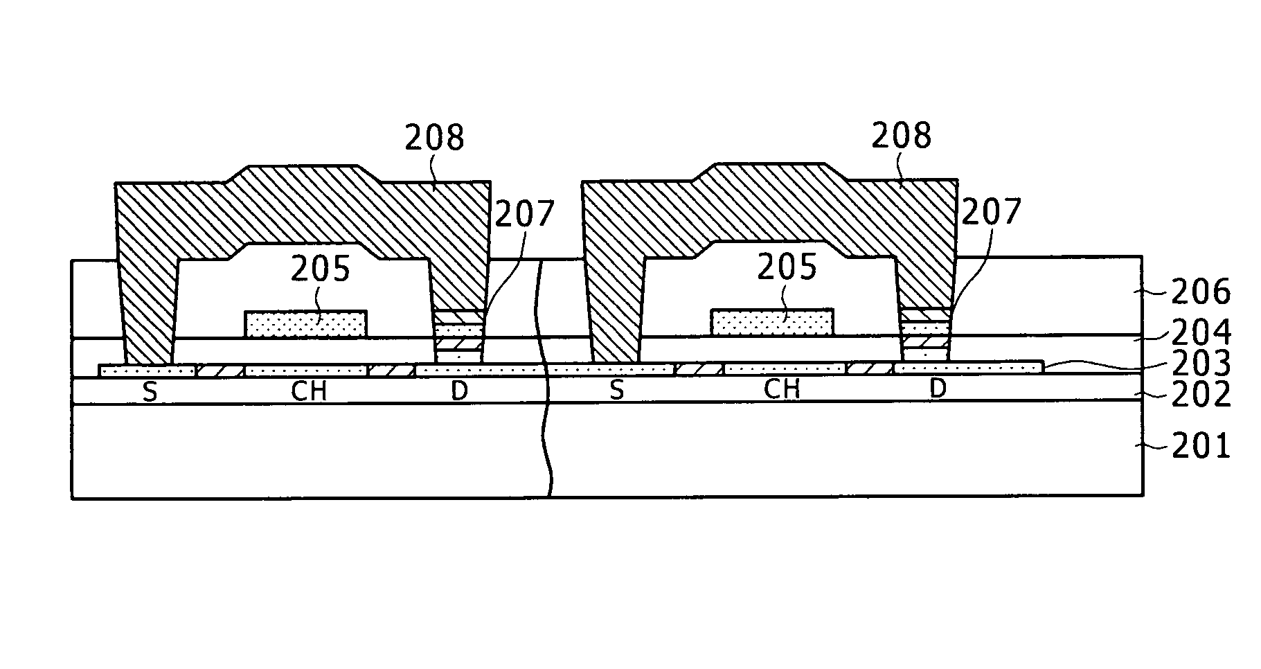
[0051]A method of manufacturing a liquid crystal display device according to a second embodiment of the present invention will be described in detail hereinafter with reference to FIGS. 4A to 4I. In the second embodiment, the memory element is formed on the side of a peripheral circuit for driving the pixel as well as on the pixel side. In each of FIGS. 4A to 4I, a process for forming a pixel portion is shown on the left-hand side, and a process for forming a peripheral circuit portion is shown on the right-hand side. However, the pixel portion and the peripheral circuit portion are simultaneously formed on an insulating substrate by utilizing the semiconductor processes. It is noted that unlike the first embodiment shown in FIGS. 3A to 3H, in the second embodiment, the TFT having a top-gate stricture is formed.

[0052]Firstly, as shown in FIG. 4A, a buffer layer 202 and an amorphous silicon layer 203 are continuously deposited on an insulating substrate 201 by ...


PUM


Abstract

Disclosed herein is a memory element, including a parallel combination of a thin film transistor; and a resistance change element, the thin film transistor including a semiconductor thin film in which a channel region, and an input terminal and an output terminal located on both sides of the channel region, respectively, are formed, and a gate electrode overlapping the channel region through an insulating film to become a control terminal, the resistance change element including one conductive layer connected to the input terminal side of the thin film transistor, the other conductive layer connected to the output terminal side of the thin film transistor, and at least one oxide film layer disposed between the one conductive layer and the other conductive layer.

Description

CROSS REFERENCES TO RELATED APPLICATIONS[0001]The present invention contains subject matter related to Japanese Patent Application JP 2008-310441 filed in the Japan Patent Office on Dec. 5, 2008 and Japanese Patent Application JP 2008-022900 filed in the Japan Patent Office on Feb. 1, 2008, the entire contents of which being incorporated herein by reference.BACKGROUND OF THE INVENTION[0002]1. Field of the Invention[0003]The present invention relates to a memory element, and more particularly to a memory element which is suitable for driving a pixel in an active matrix type liquid crystal display device. In addition, the present invention relates to an active matrix type liquid crystal display device in which such memory elements are formed in each of pixels.[0004]2. Description of the Related Art[0005]An active matrix type liquid crystal display device includes gate lines wired in rows, data lines wired in columns, and pixels disposed in portions in which both the gate lines and the...

Claims


Application Information

Patent Timeline
Patent Type & Authority Patents(United States)
IPC IPC(8): H01L45/00G11C11/00
CPCG02F1/1362G09G3/3648H01L27/24H01L27/12G09G2300/088H01L27/1214G09G2330/021H10B63/30H10B63/80H10N70/245H10N70/8833H10N70/826H10N70/8416H10N70/8836H10N70/20H10B63/00
Inventor GOSAIN, DHARAM PALTAKATOKU, MAKOTONAKAJIMA, YOSHIHARUTANAKA, TSUTOMU
Owner JAPAN DISPLAY INC
Why Eureka
Try Eureka