Ring-shaped voltage control oscillator

a voltage control and oscillator technology, applied in the field of multiphase voltage control oscillators and frequency dividers, can solve the problems of inability to provide more than, circuit topology cannot be adapted to provide vcos with odd number of phases, and vcos have proved difficult to design

Inactive Publication Date: 2012-02-14
TAIWAN SEMICON MFG CO LTD
View PDF2 Cites 12 Cited by
  • Summary
  • Abstract
  • Description
  • Claims
  • Application Information

AI Technical Summary

Problems solved by technology

However, the VCO 10 cannot provide more than two-phased oscillations, and its circuit topology cannot be adapted to provide a VCO with an odd number of phases.
While multi-phase VCOs exist in the art, these VCOs have proved difficult to design and make.
The ad hoc design solutions have tight design constraints and their topologies are not easily adapted to designs having different phase numbers.
In short, it has proved difficult to design a simple, high-performance VCO architecture that is generally applicable to any selected number of phases.
The same difficulties can be found with the frequency dividers of the prior art.

Method used


Image

  • Ring-shaped voltage control oscillator
  • Ring-shaped voltage control oscillator
  • Ring-shaped voltage control oscillator

Examples


second embodiment

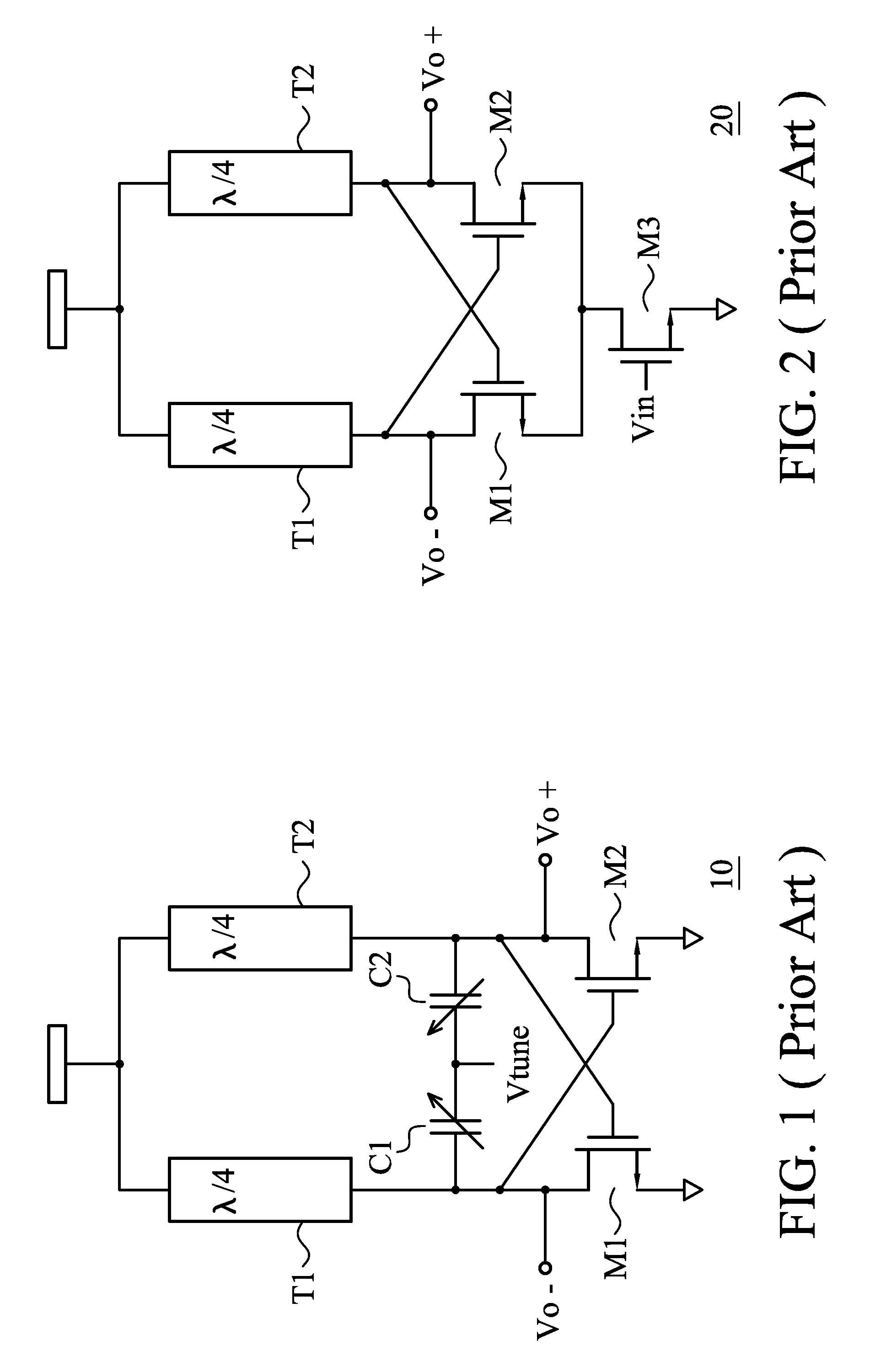
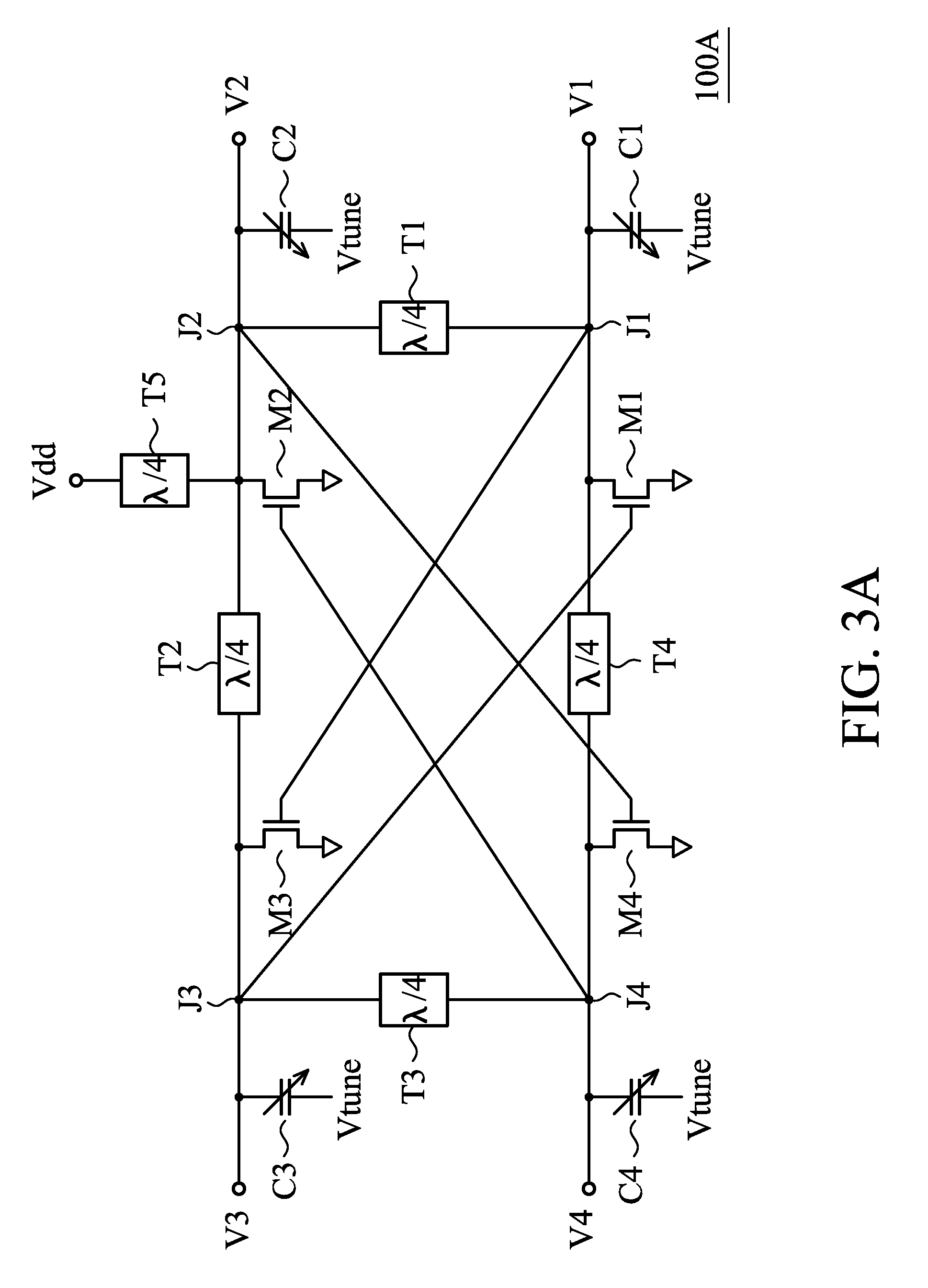
[0027]FIG. 4B is a circuit diagram of a divide-by-four injection-locked frequency divider. The circuit 150B of FIG. 4B is identical in all respects to the circuit 150A of FIG. 4A only a constant tail current source I1 is coupled to the source terminals of the transistors M1 to M4 through transistor M5.

third embodiment

[0028]FIG. 4C is a circuit diagram of a divide-by-four injection locked frequency divider. The circuit 150C is identical to the circuits 150A and 150B except that the source terminals of the transistors M1 to M4 are biased by the input voltage Vin through a sixth transmission delay line T6, which provides a delay of λ / 4.

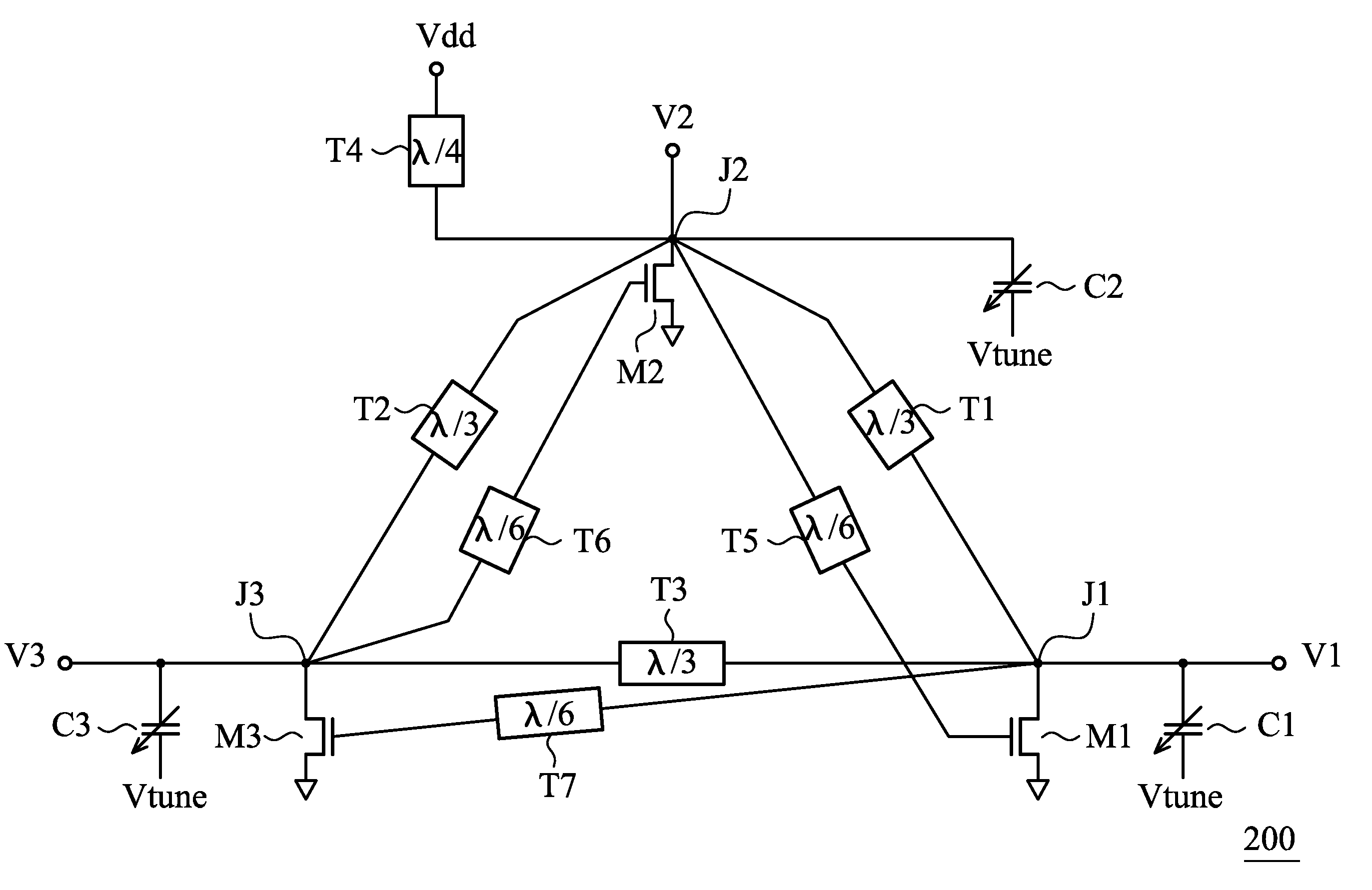
[0029]FIGS. 5 and 6 show that the circuit topology illustrated for the 4-phase VCO and for the divide-by-4 frequency divider can be easily adapted to odd phase devices. FIG. 5 shows a circuit diagram of a 3-phase VCO circuit 200. As with the 4-phase VCO circuit, the VCO circuit includes a transmission line ring having n number of λ / n delay lines connected in a ring at n junctions. Here, n is 3, so the ring includes three λ / 3 delay lines T1 to T3 with adjacent delay lines of the ring connected at junctions J1 to J3. The VCO circuit 200 also includes n number of transistors (i.e., M1 to M3) coupled to the junctions J1 to J3. The circuit 200 is DC biased from high power...


PUM


Abstract

In one embodiment, a circuit topology for use in an n-phase voltage controlled oscillator (VCO) or injection-locked frequency divider includes a transmission line ring having n transmission line delay segments connected at n junctions, where n is an integer greater than or equal to 3. Each transmission line segment provides a 1 / n wavelength signal delay between adjacent junctions. The transmission line ring is coupled to a first power supply node. Each of the junctions has a respective transistor coupled thereto, each transistor having a first source / drain terminal coupled to its respective junction, a second source / drain terminal coupled to a second power supply node, and a gate terminal, wherein the gate terminal is coupled to a signal that is ½ wavelength out-of-phase with respect to a signal at the first source / drain terminal of the transistor.

Description

FIELD OF THE INVENTION[0001]The present disclosure relates to voltage controlled oscillators (VCOs) and frequency dividers, and more specifically to multiple-phase VCOs and frequency dividers.BACKGROUND OF THE INVENTION[0002]A voltage-controlled oscillator or VCO is an electronic oscillator with its oscillation frequency controlled by a voltage input. The frequency of oscillation is varied by the applied DC voltage, while modulating signals may also be fed into the VCO to cause frequency or phase modulations.[0003]A frequency divider is an electronic circuit that takes an input signal with an input frequency and generates an output signal with an output frequency equal to the input frequency divided by some integer n.[0004]VCOs having multiple output phases form key building blocks for many wired and wireless communication systems. Frequency dividers are widely used in devices such as frequency synthesizers and as signal generators.[0005]FIG. 1 is a circuit diagram of a conventional...

Claims


Application Information

Patent Timeline
Patent Type & Authority Patents(United States)
IPC IPC(8): H03K3/03H03B5/18
CPCH03B5/1852H03L7/099
Inventor CHUNG, SHINE
Owner TAIWAN SEMICON MFG CO LTD
Why Eureka
Try Eureka