Semiconductor-chip exfoliating device and semiconductor-device manufacturing method

a technology of exfoliating device and semiconductor, applied in the direction of manufacturing tools, applications, paper/cardboard articles, etc., can solve the problem of reducing the productivity of semiconductor devices, and achieve the effect of easy exfoliation

Active Publication Date: 2012-03-27
KK TOSHIBA
View PDF47 Cites 41 Cited by
  • Summary
  • Abstract
  • Description
  • Claims
  • Application Information

AI Technical Summary

Benefits of technology

[0007]In exfoliating one semiconductor chip from the adhesive sheet, it is preferable to allow the lift-off pin to lift off chip's margins on both sides of the semiconductor chip as a target. The knocking-up of the lift-off pins against chip's margins on both sides of the chip allows the semiconductor to be exfoliated from the adhesive sheet with ease, also allowing the exfoliated chip to be broken with difficulty.
[0009]It is apt to take time and work in exchanging one lift-off unit to another one in the manufacturing process, causing the productivity of the semiconductor devices to be reduced.
[0010]Under such a situation, an object of the present invention is to provide a semiconductor-chip exfoliating device capable of making it ease to exfoliate a semiconductor chip from an adhesive sheet throughout semiconductor chips of difference sizes. Another object of the present invention is to provide a semiconductor-chip exfoliating method of exfoliating one semiconductor chip from the adhesive sheet through the use of the above semiconductor-chip exfoliating device.
[0013]With the above semiconductor-chip exfoliating device and semiconductor-device manufacturing method, by adjusting the interval between the lift-off pins corresponding to the size of a target semiconductor chip, it is possible to make the semiconductor chip easy to be exfoliated from the adhesive sheet, although there is a difference in size of the semiconductor chips adhered to the adhesive sheet.

Problems solved by technology

It is apt to take time and work in exchanging one lift-off unit to another one in the manufacturing process, causing the productivity of the semiconductor devices to be reduced.

Method used


Image

  • Semiconductor-chip exfoliating device and semiconductor-device manufacturing method
  • Semiconductor-chip exfoliating device and semiconductor-device manufacturing method
  • Semiconductor-chip exfoliating device and semiconductor-device manufacturing method

Examples


Embodiment Construction

[0021]An embodiment of the present invention will be described with reference to attached drawings.

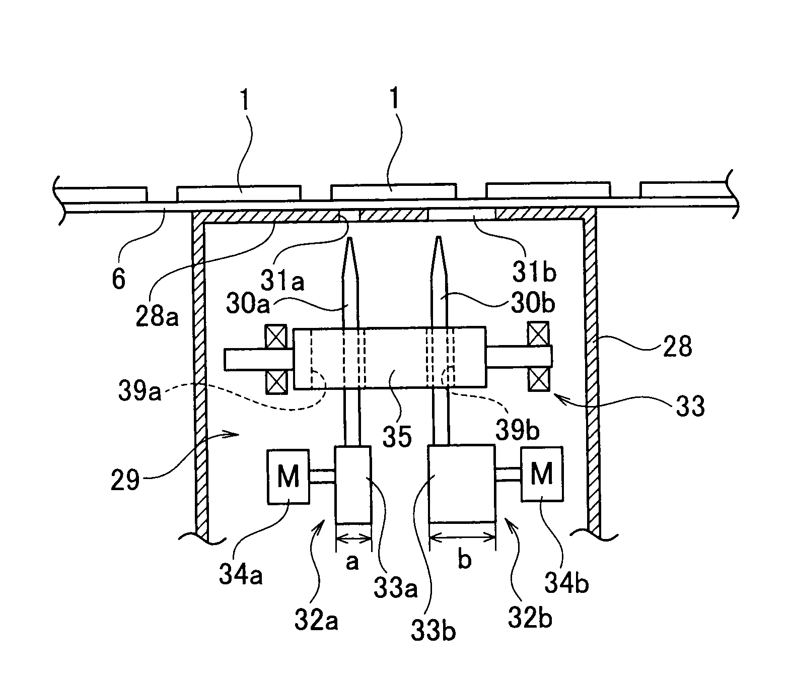
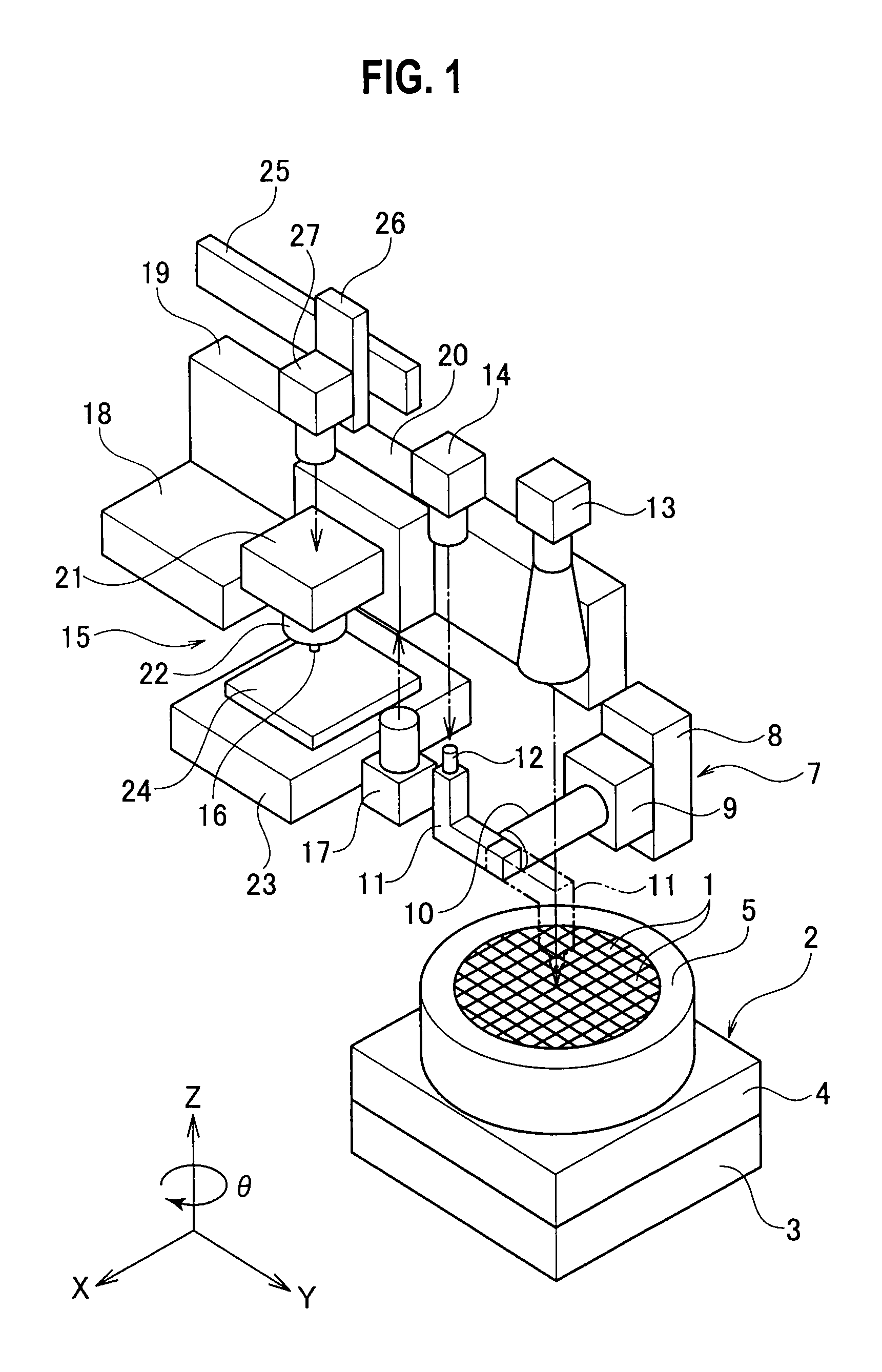
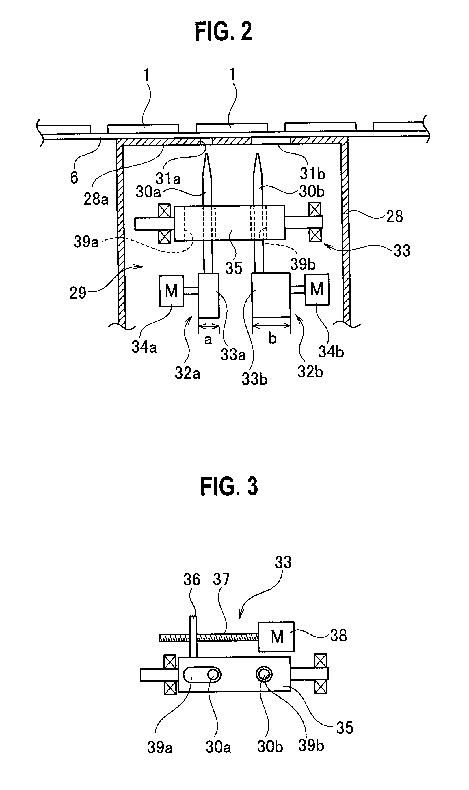
[0022]As shown in FIG. 1, a manufacturing apparatus for semiconductor devices includes a wafer stage 2 for mounting a semiconductor wafer (not shown) thereon. The wafer stage 2 comprises a base 3, a first table 4 and a second table 5 both mounted on the base 3. The second table 5 carries an adhesive sheet 6 to which a plurality of semiconductor chips 1 are adhered. The first table 4 is movable in both directions of X-axis and Y-axis. While, the second table 5 is rotatable about Z-axis in the direction of θ. For convenience of explanation, the first table 4 and the second table 5 will be referred to as “XY-axes table 4” and “θ table 5” respectively, hereinafter. The semiconductor chips 1 are produced by cutting off a piece of semiconductor wafer, which is adhered to the adhesive sheet (so-called “dicing sheet”) 6, by means of a dicing saw (not shown) vertically and horizontally. After c...


PUM

PropertyMeasurementUnit
pressureaaaaaaaaaa
timeaaaaaaaaaa
sizeaaaaaaaaaa

Abstract

A semiconductor-chip exfoliating device for exfoliating a semiconductor chip 1 from an adhesive sheet 6 is provided. The device includes a backup holder 28 for holding the adhesive sheet 6 so that semiconductor chips 1 turn upward, a pair of needle pins arranged on a backside of the holder 28 to lift off the adhesive sheet 6 from the holder 28 through through-holes 31a, 31b in the holder 28 and a sliding unit 33 arranged on the backside of the holder 28 to slide one needle pin 30b in a direction to depart from the other needle pin 30a. By the sliding unit 33, the interval between the needle pins 30a, 30b can be changed so as to cope with a variation of semiconductor chips 1, 1A.

Description

BACKGROUND OF THE INVENTION[0001]1. Field of the Invention[0002]The present invention relates to device and method for manufacturing semiconductor devices. More particularly, the invention relates to semiconductor-chip exfoliating device and method that are constructed so as to lift off an adhesive sheet having a semiconductor chip by means of lift-off pins whereby one semiconductor chip can be exfoliated from the adhesive sheet.[0003]2. Description of the Related Art[0004]Japanese Patent Publication Laid-open (heisei) No. 10-112465 discloses a prior art apparatus for manufacturing semiconductor devices. In the apparatus, a semiconductor chip adhered to an adhesive film (dicing sheet) is lifted up by lift-off pins (needle pins) to thereby exfoliate the semiconductor chip from the adhesive sheet. The so-exfoliated semiconductor chip is used to manufacture a semiconductor device.[0005]In the above-mentioned apparatus, a single semiconductor chip is lifted up by using a plurality of ne...

Claims


Application Information

Patent Timeline
Patent Type & Authority Patents(United States)
IPC IPC(8): B29C63/00
CPCH01L21/67132H01L21/6836H01L2221/68327Y10T156/1184Y10T156/1179Y10T156/11Y10T156/1983
Inventor SHIBATA, MOTOJIROUSHIJIMA, AKIRA
Owner KK TOSHIBA
Why Eureka
Try Eureka