System for displaying images including active-matrix organic light emission display

a technology of organic light emission display and active matrix, which is applied in the direction of discharge tube luminescnet screen, discharge tube/lamp details, electric discharge lamps, etc., can solve the problems of increasing fabrication cost, limited structural design current leakage at the peripheral circuit area of active matrix organic light emission display, etc., to reduce display fabrication cost, less current leakage, and improved display quality

Active Publication Date: 2012-04-03
INNOLUX CORP
View PDF12 Cites 0 Cited by
  • Summary
  • Abstract
  • Description
  • Claims
  • Application Information

AI Technical Summary

Benefits of technology

[0007]The invention utilizes a reflective layer at the peripheral circuit area of display as a light shielding layer, which is suitable for both the top emission and bottom emission AMOLEDs and does not need the color filter with black matrix as the light shielding layer. The AMOLED of the invention has less current leakage at the peripheral circuit area such that display quality can be improved. Moreover, fabrication of the reflective layer can be integrated with the active-matrix array process to reduce display fabrication costs.

Problems solved by technology

As a result, current leakages occur at the peripheral circuit area of the active-matrix organic light emission displays.
Although the peripheral circuit area of FIG. 3 has a black matrix as a light shielding layer, the black matrix is only suitable for the top emission AMOLED as a light shielding layer.
Moreover, the AMOLED must have a color filter such that structural design thereof is limited and fabrication cost is increased.

Method used


Image

  • System for displaying images including active-matrix organic light emission display
  • System for displaying images including active-matrix organic light emission display
  • System for displaying images including active-matrix organic light emission display

Examples


Embodiment Construction

[0018]The following description is of the best-contemplated mode of carrying out the invention. The description is provided for illustrating the general principles of the invention and is not meant to be limiting. The scope of the invention is best determined by reference to the appended claims.

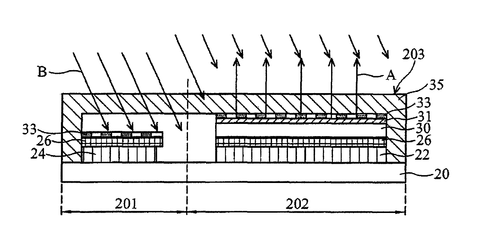
[0019]In order to reduce current leakage at the peripheral circuit area of the display and improve display quality, a reflective layer is disposed between a light emission plane and a peripheral circuit area of an active-matrix organic light emission display. The reflective layer fabrication can be integrated with current active-matrix array processes. The reflective layer can be formed by general array processes without extra processes and materials, such that fabrication cost of the display can be reduced. Moreover, the reflective layer structure can be used in both top emission and bottom emission AMOLEDs.

[0020]Referring to FIG. 4, a cross section of a top emission AMOLED according to an e...


PUM


Abstract

A system for displaying images is provided, including an active-matrix organic light emission display. The active-matrix organic light emission display comprises an active-matrix array on a display area of an array substrate, a peripheral circuit on a peripheral area of the array substrate, a reflective layer on the peripheral area of the array substrate, between a light emission plane and the peripheral circuit and covering the peripheral circuit, an organic light emission layer on the active-matrix array and a cover layer over the organic light emission layer, covering the display area and the peripheral area.

Description

FIELD OF THE INVENTION[0001]The invention relates to a system for displaying image including an active-matrix organic light emission display, and more particularly to an active-matrix organic light emission display having a light shielding structure at a peripheral circuit area.DESCRIPTION OF THE RELATED ART[0002]Recently, liquid crystal displays or active-matrix organic light emission displays (AMOLED) have been applied widely to display elements of various products. Displays need a peripheral circuit to be disposed on the panel. For panel designs of active-matrix organic light emission displays, thin film transistors in the peripheral circuit are easily illuminated by external light to produce photoelectric effect. As a result, current leakages occur at the peripheral circuit area of the active-matrix organic light emission displays.[0003]The conventional active-matrix organic light emission display includes a bottom emission AMOLED and a top emission AMOLED. The cross sections of...

Claims


Application Information

Patent Timeline
Patent Type & Authority Patents(United States)
IPC IPC(8): H01L51/52
CPCH01L27/3272H10K59/126
Inventor CHAN, CHUAN-YILIU, PING-LINPENG, DU-ZEN
Owner INNOLUX CORP
Why Eureka
Try Eureka