Dielectric material forming methods and enhanced dielectric materials

a technology of dielectric materials and forming methods, applied in the direction of coatings, chemical vapor deposition coatings, semiconductor devices, etc., can solve the problems of exhibiting a high k and suffering the disadvantage of exhibiting an unacceptable leakage current, and achieve the effect of less current leakag

Inactive Publication Date: 2006-05-30
CONVERSANT INTPROP MANAGEMENT INC +1
View PDF5 Cites 3 Cited by
  • Summary
  • Abstract
  • Description
  • Claims
  • Application Information

AI Technical Summary

Benefits of technology

[0007]In another aspect of the invention, a dielectric material forming method can include chemisorbing a first dielectric material on a substrate, chemisorbing a second dielectric material on the first material, one of the first and second materials comprising oxygen and a metal element, and forming an enhanced dielectric material containing the first and second materials. The enhanced dielectric material can exhibit a dielectric constant greater than the first dielectric material. As an example, the metal element can be a Group IB to VIIIB element, such as titanium or zirconium. Also, the one of the materials can further contain a different metal element. The enhanced dielectric material may further exhibit less current leakage than the first diectric material.

Problems solved by technology

Often, processing limitations and / or cost limitations impact the ability to provide a desirably high K. Some dielectric materials, although exhibiting a high K may suffer the disadvantage of exhibiting an unacceptable leakage current.

Method used


Image

  • Dielectric material forming methods and enhanced dielectric materials
  • Dielectric material forming methods and enhanced dielectric materials
  • Dielectric material forming methods and enhanced dielectric materials

Examples


Embodiment Construction

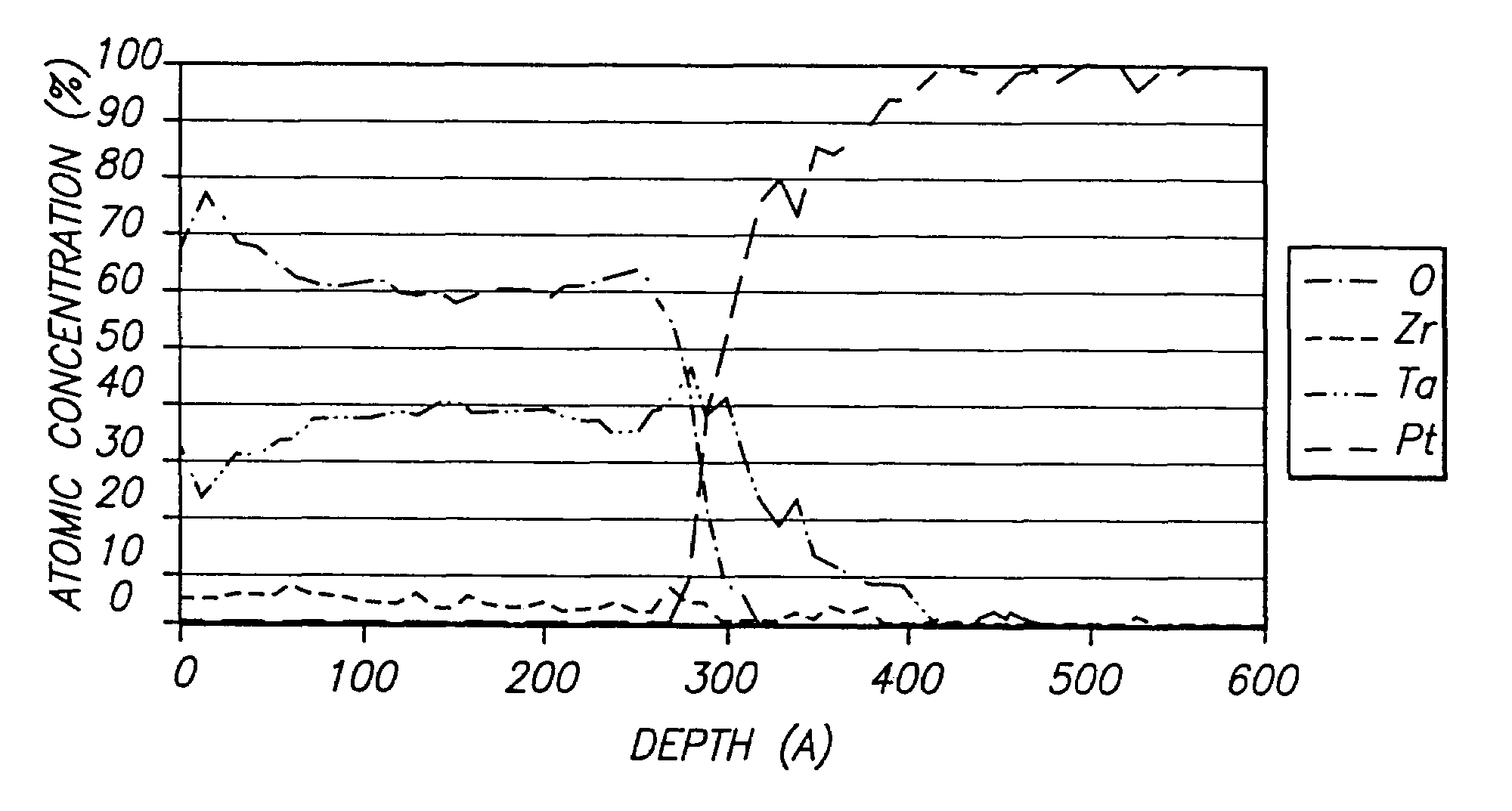
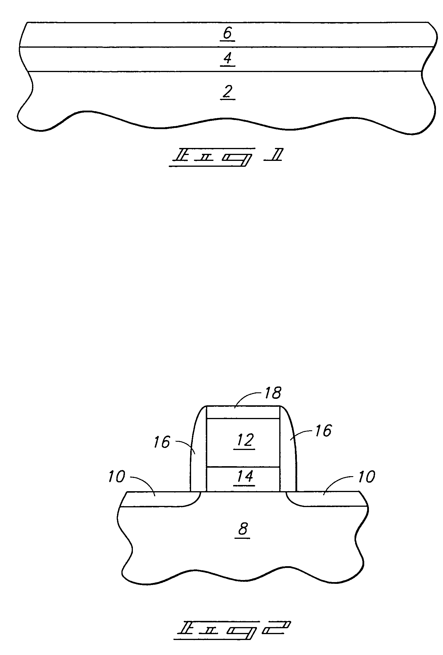
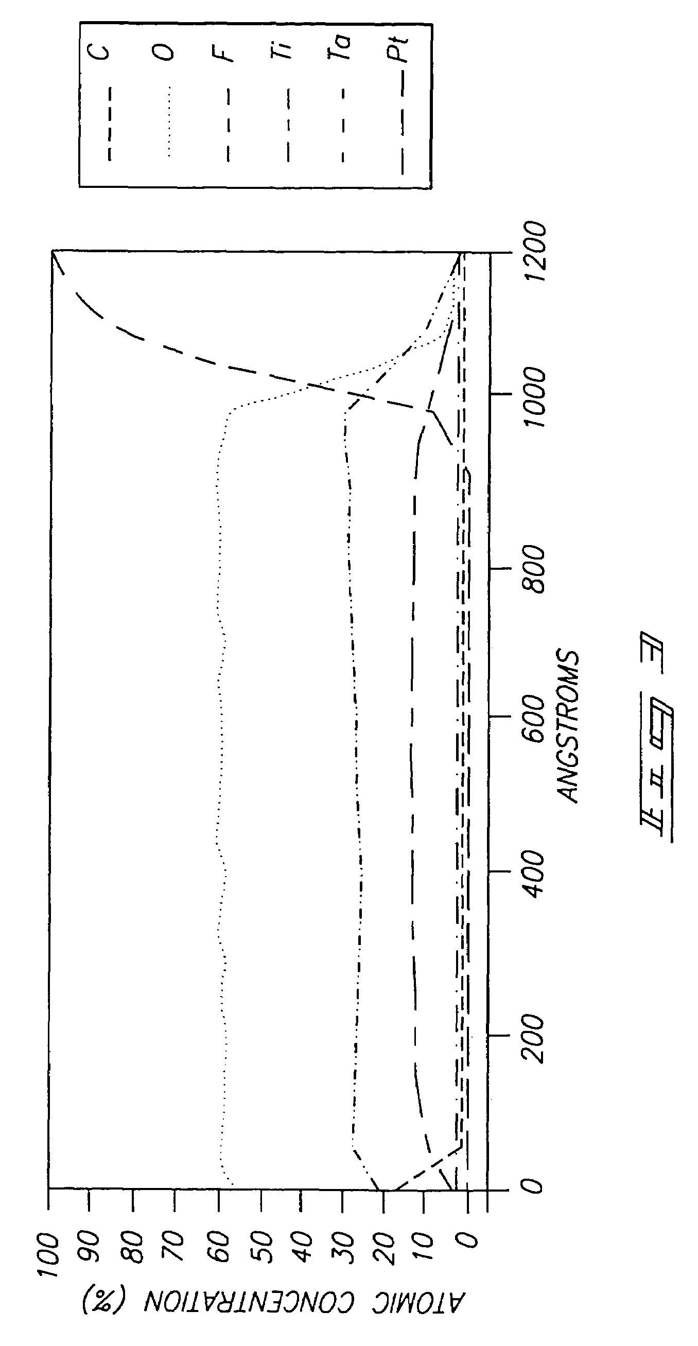
[0016]Atomic layer deposition (ALD) involves formation of successive atomic layers on a substrate. Such layers may comprise an epitaxial, polycrystalline, amorphous, etc. material. ALD may also be referred to as atomic layer epitaxy, atomic layer processing, etc. Further, the invention may encompass other deposition methods not traditionally referred to as ALD, for example, chemical vapor deposition (CVD), but nevertheless including the method steps described herein. The deposition methods herein may be described in the context of formation on a semiconductor wafer. However, the invention encompasses deposition on a variety of substrates besides semiconductor substrates.

[0017]In the context of this document, the term “semiconductor substrate” or “semiconductive substrate” is defined to mean any construction comprising semiconductive material, including, but not limited to, bulk semiconductive materials such as a semiconductive wafer (either alone or in assemblies comprising other ma...


PUM

PropertyMeasurementUnit
pressureaaaaaaaaaa
thicknessaaaaaaaaaa
thicknessaaaaaaaaaa

Abstract

A dielectric material forming method includes forming a first monolayer and forming a second monolayer on the first monolayer, one of the first and second monolayers comprising tantalum and oxygen and the other of the first and second monolayers comprising oxygen and another element different from tantalum. A dielectric layer can be formed containing the first and second monolayers. The dielectric layer can exhibit a dielectric constant greater than the first monolayer. The another element can include a Group IB to VIIIB element, such as titanium and / or zirconium. The forming of the first and second monolayer can include atomic layer depositing. A dielectric material can include first and second chemisorbed materials, the second material containing oxygen and a Group IB to VIIIB element and the dielectric material exhibiting a dielectric constant greater than the first chemisorbed material. The dielectric material can further exhibit less current leakage than the first material.

Description

[0001]This patent resulted from a divisional application of U.S. patent application Ser. No. 09 / 945,393, filed on Aug. 30, 2001.TECHNICAL FIELD[0002]This invention relates to dielectric material forming methods and dielectric materials.BACKGROUND OF THE INVENTION[0003]Dielectric materials are used in a wide variety of apparatuses including, but not limited to semiconductor-based electronic devices and other electronic devices. For example, a dielectric material can form a dielectric layer in a capacitor as shown in FIG. 1. The capacitor of FIG. 1 includes a lower electrode 2 underlying a dielectric layer 4 and an upper electrode 6. Generally, a capacitor can be formed smaller and perform better when the dielectric constant “K” of dielectric layer 4 is maximized. Often, processing limitations and / or cost limitations impact the ability to provide a desirably high K. Some dielectric materials, although exhibiting a high K may suffer the disadvantage of exhibiting an unacceptable leakag...

Claims


Application Information

Patent Timeline
Patent Type & Authority Patents(United States)
IPC IPC(8): H01L21/316C23C16/40C23C16/44C23C16/455H01L21/28H01L29/51
CPCC23C16/405C23C16/45531H01L21/28185H01L29/517H01L21/31604H01L29/513H01L21/28194H01L21/31683H01L21/0228H01L21/02183
Inventor MARSH, EUGENE P.
Owner CONVERSANT INTPROP MANAGEMENT INC
Why Eureka
Try Eureka