Transistor and method of making the same

A manufacturing method and transistor technology, applied in semiconductor/solid-state device manufacturing, semiconductor devices, electrical components, etc., can solve the problems of left and right damage, leakage, and affecting the electrical performance of transistors, and achieve the effect of less current leakage

Active Publication Date: 2017-09-22
SEMICON MFG INT (SHANGHAI) CORP
View PDF3 Cites 0 Cited by
  • Summary
  • Abstract
  • Description
  • Claims
  • Application Information

AI Technical Summary

Problems solved by technology

[0005] Dry etching is a method of etching using plasma. During the process of forming the stack structure 6 by dry etching, the plasma will damage the left and right sides of the stack structure 6 exposed to the plasma environment. so as to affect the electrical performance of the transistor
The transistor formed by the above method is detected and found that both sides 2a of the high-K gate dielectric layer 2 in the stacked structure 6 will have a problem of leakage current due to the damage of the plasma, and then the current switching ratio of the transistor (Ion / Ioff), GIDL (Gate Induced Drain Leakage) and other performance degradation, resulting in higher current leakage at the gate of the transistor

Method used


Image

  • Transistor and method of making the same
  • Transistor and method of making the same
  • Transistor and method of making the same

Examples


Embodiment Construction

[0030] The technical solution of the present invention will be described clearly and completely through specific embodiments below in conjunction with the accompanying drawings. Apparently, the described embodiments are only a part of the possible implementation modes of the present invention, not all of them. According to these embodiments, all other implementation manners that can be obtained by those skilled in the art without creative efforts belong to the protection scope of the present invention.

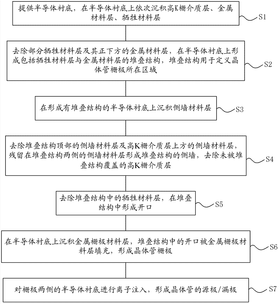
[0031] figure 2 It is a fabrication flowchart of the transistor in the embodiment of the fabrication method of the transistor of the present invention. Such as figure 2 As shown, the method includes the following steps:

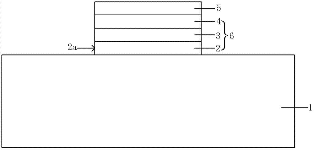
[0032] S1: Provide a semiconductor substrate, and sequentially deposit a high-K gate dielectric layer, a metal material layer, and a sacrificial material layer on the semiconductor substrate.

[0033] S2: removing part of the sacrificial material layer a...


PUM


Abstract

The invention provides a transistor and a manufacturing method thereof. The method comprises the following steps: providing a semiconductor substrate; sequentially depositing a high-K gate dielectric layer, a metal material layer, and a sacrificial material layer on the semiconductor substrate; removing part of the sacrificial material layer and The metal material layer directly below it forms a stacked structure including a sacrificial material layer and a metal material layer on the semiconductor substrate, and the stacked structure is used to define the area where the gate of the transistor is located; deposit sidewalls on the semiconductor substrate formed with the stacked structure Material layer: remove the stacked structure and the sidewall material layer above the high-K gate dielectric layer, the sidewall material layers remaining on both sides of the stacked structure form sidewalls of the stacked structure, and remove the high-K gate dielectric layer not covered by the stacked structure. The high-K gate dielectric layer in the formed transistor does not cause leakage current, improves the current switching ratio of the transistor, GIDL and other performances, and causes less current leakage at the gate of the transistor.

Description

technical field [0001] The invention relates to the field of semiconductor manufacturing, in particular to a transistor and a manufacturing method thereof. Background technique [0002] A common trend in modern integrated circuit fabrication is to produce transistors with very small feature sizes. Many problems have arisen with transistors as their dimensions have become smaller and smaller. For example, a very thin gate dielectric layer causes high gate current leakage; in addition, the material of the transistor gate is generally polysilicon, but the polysilicon gate often causes problems such as polysilicon depletion or boron penetration effect, which will affect the transistor. performance. [0003] Metal is another material used to make transistor gates, and gates made of metal have many advantages over polysilicon gates. For example, metal allows excellent current flow and has fewer voltage drain problems than polysilicon. [0004] A manufacturing method of a trans...

Claims


Application Information

Patent Timeline
Patent Type & Authority Patents(China)
IPC IPC(8): H01L21/336H01L29/78H01L29/423
Inventor 平延磊何其旸
Owner SEMICON MFG INT (SHANGHAI) CORP
Why Eureka
Try Eureka