A van der Waals heterojunction device and its preparation method and application

A heterojunction and device technology, applied in semiconductor/solid-state device manufacturing, semiconductor devices, electrical components, etc., to achieve excellent photovoltaic performance

Active Publication Date: 2022-02-08
THE NAT CENT FOR NANOSCI & TECH NCNST OF CHINA
View PDF2 Cites 0 Cited by
  • Summary
  • Abstract
  • Description
  • Claims
  • Application Information

AI Technical Summary

Problems solved by technology

Nevertheless, these heterojunction devices usually exhibit fixed conduction properties, and van der Waals heterojunction devices with dynamically adjustable conduction polarity have not yet been reported.

Method used


Image

  • A van der Waals heterojunction device and its preparation method and application
  • A van der Waals heterojunction device and its preparation method and application
  • A van der Waals heterojunction device and its preparation method and application

Examples


Embodiment 1

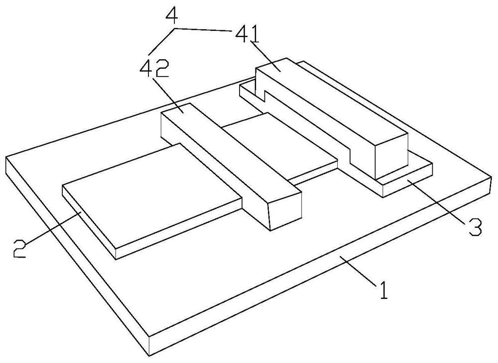
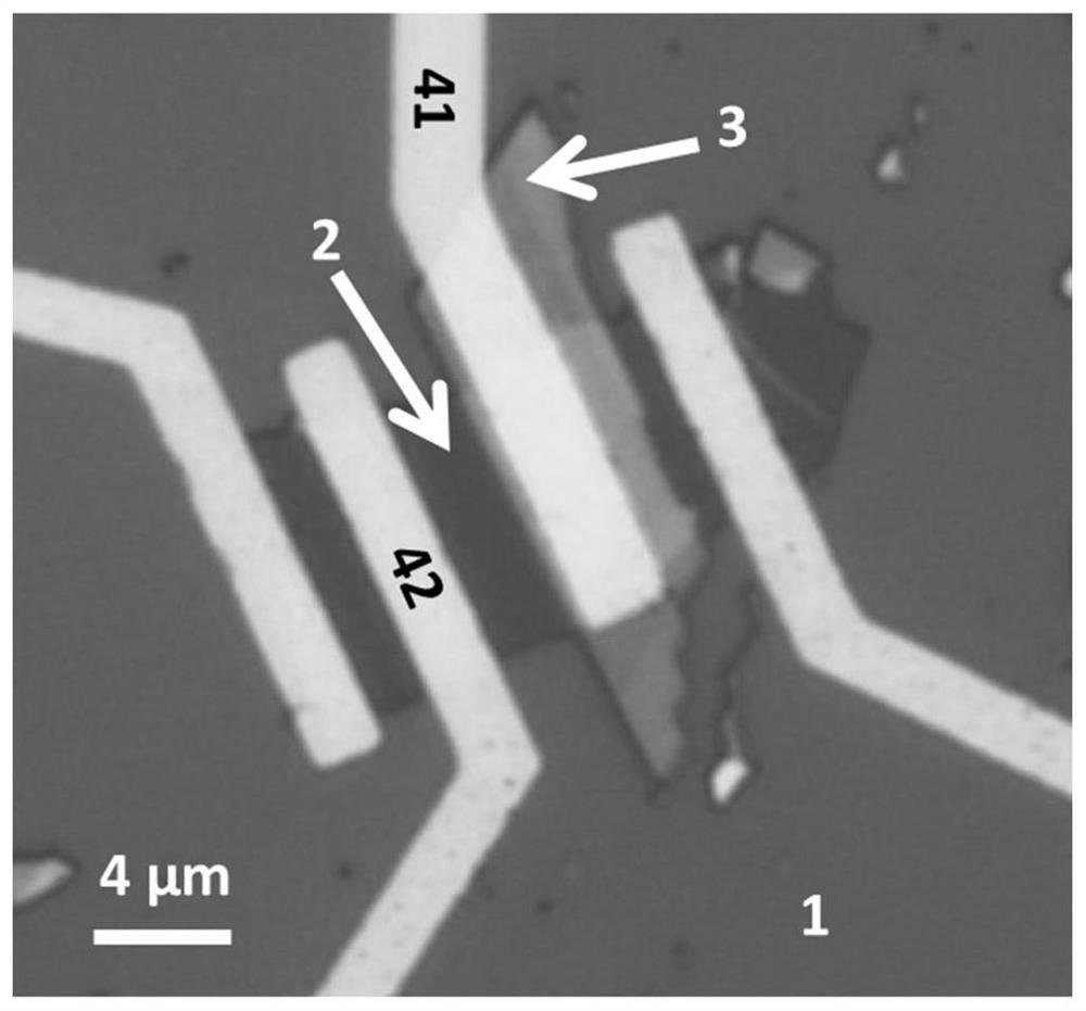
[0038] This embodiment provides a van der Waals heterojunction device, and its structural schematic diagram is as follows figure 1 As shown, it includes substrate 1, molybdenum ditelluride nanosheets 2, molybdenum disulfide nanosheets 3 and metal electrodes 4 arranged in sequence from bottom to top, and the cross-sectional area of ​​molybdenum ditelluride nanosheets 2 is larger than that of molybdenum disulfide nanosheets 3 cross-sectional area.

[0039] In this embodiment, the substrate 1 is a silicon substrate with 300nm thick silicon dioxide; the thickness of the molybdenum ditelluride nanosheet 2 is 6.4nm, the length is 17.4 μm, and the width is 7.5 μm; the thickness of the molybdenum disulfide nanosheet 3 is It is 13.7nm, the length is 11.4 μm, and the width is 4.2 μm; the metal electrode 4 includes a source electrode 41 and a drain electrode 42, and the source electrode 41 is arranged on the overlapping region of the molybdenum disulfide nanosheet 3 and the molybdenum di...

Embodiment 2

[0050] This embodiment provides a van der Waals heterojunction device, comprising a substrate, molybdenum ditelluride nanosheets, molybdenum disulfide nanosheets, and metal electrodes arranged in sequence from bottom to top, and the cross-sectional area of ​​the molybdenum ditelluride nanosheets is greater than two Cross-sectional area of ​​MoS nanosheets.

[0051] In this embodiment, the substrate is a silicon substrate with 300nm thick silicon dioxide; the thickness of molybdenum ditelluride nanosheets is 4.1nm, the length is 21.9 μm, and the width is 6.4 μm; the thickness of molybdenum disulfide nanosheets is 16.1nm , the length is 16.4 μm, and the width is 6.2 μm; the metal electrode includes a source and a drain, the source is set on the overlapping area of ​​the molybdenum disulfide nanosheet and the molybdenum ditelluride nanosheet, and the drain is set on the molybdenum ditelluride nanosheet On the non-overlapping area of ​​the chip, the source and drain electrodes are...


PUM

PropertyMeasurementUnit
thicknessaaaaaaaaaa
thicknessaaaaaaaaaa
lengthaaaaaaaaaa

Abstract

The invention provides a van der Waals heterojunction device, comprising a base, a molybdenum ditelluride nanosheet, a molybdenum disulfide nanosheet and a metal electrode sequentially arranged from bottom to top, and the cross-sectional area of ​​the molybdenum ditelluride nanosheet is larger than The cross-sectional area of ​​the molybdenum disulfide nanosheets. The van der Waals heterojunction device of the invention can realize the dynamic adjustment of the conduction polarity. Under different bias conditions, field-effect transistors based on this van der Waals heterojunction device can achieve bipolar and N-type conduction polarity, respectively, and exhibit an ultrahigh current switching ratio (~10 7 ), current rectification ratio (~10 6 ) and excellent photovoltaic performance, which can be applied in new two-dimensional electronic and optoelectronic devices.

Description

technical field [0001] The invention relates to the technical field of semiconductor nanomaterials, in particular to a van der Waals heterojunction device and its preparation method and application. Background technique [0002] Two-dimensional materials have attracted more and more attention from researchers because of their atomic-level ultra-thin thickness and no surface dangling bonds. Controllable conductive properties (such as conductive polarity) are the prerequisite for their practical application. . At this stage, due to the existence of a large number of interface states, there are still many challenges in the regulation of the conductive properties of two-dimensional materials. It can be effectively regulated by surface chemical doping, but this will increase the complexity of the device fabrication process and have problems such as easy degradation of performance. More importantly, this method is irreversible and cannot achieve dynamic adjustment of the conduct...

Claims


Application Information

Patent Timeline
Patent Type & Authority Patents(China)
IPC IPC(8): H01L29/06H01L21/04H01L29/778
CPCH01L29/0646H01L29/778H01L29/7786H01L21/04
Inventor 何军尹蕾程瑞清王振兴王峰
Owner THE NAT CENT FOR NANOSCI & TECH NCNST OF CHINA
Why Eureka
Try Eureka