Rhenium disulfide-based field effect transistor and manufacturing method thereof

A rhenium disulfide and field effect transistor technology, which is applied to the field effect transistor based on rhenium disulfide and its manufacturing field, can solve the problems of reducing device length, process and cost constraints, and achieves the effect of controlling the size of the drain-source current

Pending Publication Date: 2021-09-24
LANZHOU UNIVERSITY
View PDF6 Cites 0 Cited by
  • Summary
  • Abstract
  • Description
  • Claims
  • Application Information

AI Technical Summary

Problems solved by technology

[0002] With the rapid development of semiconductor integrated circuits, the feature size of integrated circuits can be reduc

Method used


Image

  • Rhenium disulfide-based field effect transistor and manufacturing method thereof
  • Rhenium disulfide-based field effect transistor and manufacturing method thereof
  • Rhenium disulfide-based field effect transistor and manufacturing method thereof

Examples


Embodiment 1

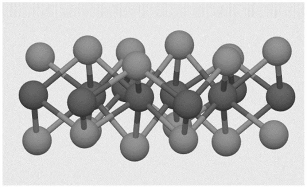
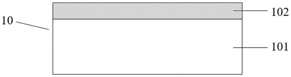
[0028] An field effect tube based on a disulfide-based ruthenium comprising a substrate 10, the substrate 10 comprising a silicon substrate 101 and a oxide layer 102 grown on the silicon substrate 101, the oxide layer 102 Elegly etching there is a sulfide trench 11, the field effect tube further comprising a drain electrode 12 grown in a source leak contact zone, covering the gate oxide layer 13 of the sulfide rutes 11 and at the bottom of the silicon substrate 101. Metal lead 15, the gate electrode 14 is grown on the gate oxide layer 13, which includes a CR electrode 121 and the Au electrode 122 disposed over the oxide layer 102. The silicon substrate 101 is p-type heavy doping, and the doped type is p-type heavy doping (P +), and the impurities may be boron and / or aluminum and / or indium, in the first embodiment, The oxide layer 102 is a silica film having a thickness of 50 to 300 nm. The silicon substrate 101 has a doping concentration greater than 10 19 / cm -3 And less tha...

Embodiment 2

[0036] In the present embodiment, the oxide layer 102 is a silica film having a thickness of 50 to 300 nm. The silicon substrate 101 has a doping concentration of 0. The gate oxide layer 13 has a thickness of from 30 to 50 nm, and the thickness of the sulfide trench 11 is from 5 to 10 nm, and the thickness of the CR electrode 121 is 5-10 nm, and the thickness of the Au electrode 122 is 80- 100nm.

[0037] The specific properties of the field effect tube described in Example 2 are:

[0038] Control V DS When 100mV is unchanged, the back gate voltage V is BG Size from -20V to 10V, i DS From 10 -14 A magnitude change to 10 -8 A level, at this time, the switch current is 10 6 When further increasing V DS , Switch current ratio is greater than 10 6 . It can be seen that when the silicon substrate 101 is not doped, the back gate control voltage V BG The value is larger than the doping, and the recombination of silicon substrate can reduce the voltage.

Embodiment 3

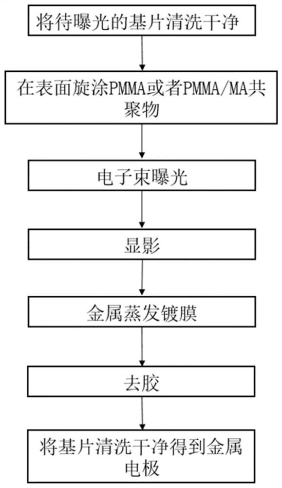
[0040] The method of manufacturing a field effect tube based on a sulfide ruthenium according to the present invention, such as Figure 9 As shown, the specifically includes the steps of:

[0041] A substrate 10 is supplied, the substrate comprising a silicon substrate 101, a layer of oxide layer 102 is grown on the silicon substrate 101, and then the substrate 10 is cleaned, and the surface is dry and flat, no impurities.

[0042] A particular preparation method of the silicon substrate 101 is: injecting boron ions to silicon substrate by a high energy ion implantation machine, doping concentration is 10 19 -10 21 / cm 3 The ion beam energy is 300 keV, annealing at a high temperature for 20-30 min, resulting in a P-type retaining silicon substrate 101, and the substrate 10 is schematically image 3 Indicated. The present invention is used as a back gate with a heavy doped p-type silicon substrate, by adjusting the back gate voltage V. BG And a grid voltage V TG To change the conduc...


PUM

PropertyMeasurementUnit
Thicknessaaaaaaaaaa
Thicknessaaaaaaaaaa
Thicknessaaaaaaaaaa

Abstract

The invention relates to a rhenium disulfide-based field effect transistor and a manufacturing method thereof, the rhenium disulfide-based field effect transistor comprises a substrate, the substrate comprises a silicon substrate and an oxide layer growing on the silicon substrate, a rhenium disulfide channel is etched on the oxide layer, the field effect transistor further comprises a drain-source electrode growing in the source-drain contact region, a gate oxide layer covering the rhenium disulfide channel and a metal lead located at the bottom of the silicon substrate, a gate electrode grows on the gate oxide layer, and the drain-source electrode comprises a Cr electrode and an Au electrode which are sequentially located on the oxide layer. The field effect transistor has a high switching current ratio, the short channel effect caused by device size reduction is effectively reduced, and meanwhile, the structure of the top gate and the back gate is also beneficial to regulation and control of source and drain currents.

Description

Technical field [0001] The present invention belongs to the field of integrated circuits, and more particularly to field effect tubes based on sulfide oxide and its manufacturing method thereof. Background technique [0002] With the rapid development of the semiconductor integrated circuit, the integrated circuit feature size can be reduced to the nanometer scale, but further reduction of the length of the device is severely limited by the process and cost. When the size breaks through a certain node, the quantum effect of the device will not be ignored. Inventive content [0003] SUMMARY OF THE INVENTION It is an object of the present invention to overcome the shortcomings of the prior art, and propose a field effect tube based on disulfide and its manufacturing method thereof. [0004] An field effect tube based on a disulfide-based ruthenium, comprising a substrate comprising a silicon substrate and a oxide layer grown on the silicon substrate, etching on the oxide layer The...

Claims


Application Information

Patent Timeline
IPC IPC(8): H01L29/778H01L29/24H01L29/423H01L21/336
CPCH01L29/778H01L29/24H01L29/42364H01L29/4232H01L29/66007
Inventor 赵桂娟黄河源邢树安吕秀睿茆邦耀刘贵鹏
Owner LANZHOU UNIVERSITY
Why Eureka
Try Eureka