
Amorphous oxide thin film for thin film transistor channel layer and manufacturing method thereof

A technology of amorphous oxide and thin film transistors, which is applied in the direction of transistors, coatings, metal material coating processes, etc., can solve the problems of high price, difficult mining, accelerated In consumption, etc., to reduce oxygen vacancies, suppress electron concentration, The effect of reducing the off-state current

Inactive Publication Date: 2013-07-24
ZHEJIANG UNIV
View PDF3 Cites 0 Cited by
  • Summary
  • Abstract
  • Description
  • Claims
  • Application Information

AI Technical Summary

Problems solved by technology

However, for IGZO TFT, there is a big disadvantage that the prices of these two elements, In and Ga, are high.
In particular, the In element has very few reserves on the earth, and it exists as an associated ore of Zn, Sn and other elements, and it is very difficult to mine.
Moreover, In is widely used in transparent conductive thin film ITO, which accelerates the consumption of In. Some researchers predict that In resources will be exhausted in the next few decades.

Method used


Image

  • Amorphous oxide thin film for thin film transistor channel layer and manufacturing method thereof
  • Amorphous oxide thin film for thin film transistor channel layer and manufacturing method thereof
  • Amorphous oxide thin film for thin film transistor channel layer and manufacturing method thereof

Examples


example 1

[0024] 1) SnO with a purity of 99.99% 2 , SiO 2 and ZnO powder as raw materials, weighed according to the atomic ratio Si:Zn:Sn=0.06:1:1, and weighed SiO 2 0.3605 g, ZnO 8.139 g, SnO 2 15.07 g, the weighed powder was poured into a ball mill jar equipped with agate balls and ethanol, and ball milled on a ball mill for 48 hours to make the powder fine and evenly mixed. Then the raw materials are separated, dried at 80°C for 24 hours, added with a binder, ground, and pressed into a disc-shaped embryo body with a diameter of about 3 cm and a thickness of 3 mm. Put the formed green body into the sintering furnace and sinter at 1200 °C for 12 hours to obtain the required ceramic target.

[0025] 2) Using the pulsed laser deposition method, using the ceramic target in step 1) as the target, a layer of amorphous oxide film is deposited on the cleaned substrate. The deposition conditions are: the distance between the glass substrate and the target is 55 mm , the vacuum of the gro...

example 2

[0030] 1) SnO with a purity of 99.99% 2 , SiO 2 and ZnO powder as raw materials, weighed according to the atomic ratio Si:Zn:Sn=0.14:1:1, and weighed SiO 20.8413 g, ZnO 8.139 g, SnO 2 15.07 g, the weighed powder was poured into a ball mill jar equipped with agate balls and ethanol, and ball milled on a ball mill for 48 hours to make the powder fine and evenly mixed. Then the raw materials were separated, dried at 80°C for 24 hours, added with a binder, ground, and pressed into a disc shape with a diameter of about 3 cm and a thickness of 3 mm. Put the formed green body into the sintering furnace and sinter at 1200 °C for 12 hours to obtain the required ceramic target.

[0031] 2) Using the pulsed laser deposition method, using the ceramic target in step 1) as the target, a layer of amorphous oxide film is deposited on the cleaned substrate. The deposition conditions are: the distance between the glass substrate and the target is 55 mm , the vacuum of the growth chamber wa...


PUM

PropertyMeasurementUnit
surface roughnessaaaaaaaaaa

Abstract

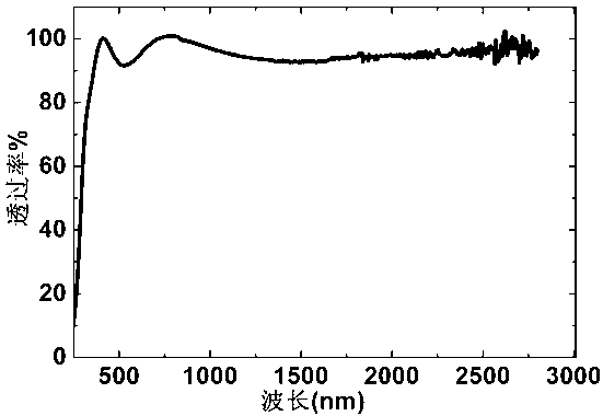
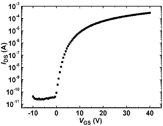
The invention discloses an amorphous oxide thin film for a thin film transistor channel layer and a manufacturing method of the amorphous oxide thin film for the thin film transistor channel layer. The chemical formula is that SixZnSnO2x+3, 0.06<=x<=0.14. The surface roughness RMS is less than 2nm and the carrier concentration is 1014-1017cm<-3>. A pulsed laser deposition method is adopted for preparation and the target material is obtained by mixing and sintering of SiO2 powder, ZnO powder and SnO2 powder with purity more than 99.9%. The atomic ratio of the SiO2 powder, the ZnO powder and the SnO2 powder is Si: Zn: Sn=0.06-0.14:1:1. The growth temperature of the thin film is 25 DEG C-400 DEG C. The amorphous oxide thin film for the thin film transistor channel layer has the advantages of being high in grade of transparency in a visible region, low in roughness of the surface, high in mobility ratio, low in preparing temperature, ample in raw material reserve volume and low in cost.

Description

technical field [0001] The invention relates to an amorphous oxide film and a preparation method thereof, in particular to an amorphous oxide film used as a channel layer of a thin film transistor and a preparation method thereof. Background technique [0002] At present, flat panel display technology is developing in the direction of high resolution, large size, light weight, transparency, and bendability, which undoubtedly puts forward higher requirements for the performance of TFT (thin film transistor), the core of the flat panel display drive circuit. . However, the α-Si TFT widely used in industry can no longer meet the requirements of next-generation high-performance flat panel display, mainly because of the low mobility of α-Si (<1 cm 2 V -1 the s -1 ), sensitive to visible light, need to add a mask layer, low pixel aperture ratio, and complicated preparation process. Therefore, TFT technology is one of the main links restricting the development of information...

Claims


Application Information

Patent Timeline
Patent Type & Authority Applications(China)
IPC IPC(8): H01L29/786C23C14/08C23C14/34
Inventor 吕建国吴传佳叶志镇张杰吴萍陈凌翔江庆军孙汝杰
Owner ZHEJIANG UNIV
Learn More