An Asymmetric Reconfigurable Field Effect Transistor

A field-effect transistor, asymmetric technology, applied in the field of reconfigurable field-effect transistors, can solve the problems of shortening the operation delay of logic gates, low open-state driving current of reconfigurable transistors, etc., and achieves strong logic processing capability and clock frequency improvement. , the effect of shortening the switching delay time

Active Publication Date: 2020-08-04
EAST CHINA NORMAL UNIV +1
View PDF9 Cites 0 Cited by
  • Summary
  • Abstract
  • Description
  • Claims
  • Application Information

AI Technical Summary

Problems solved by technology

[0006] The purpose of the present invention is to solve the problem that the open-state drive current of the existing general symmetrical structure reconfigurable transistor is low, in order to improve the open current of the device, shorten the switching time of the transistor, and shorten the operation delay of the logic gate, propose an asymmetric The reconfigurable field effect transistor of the symmetric structure can realize the improvement of the N-type and P-type leakage currents of the device under the same order of magnitude as the leakage current of the N-type and P-type devices. Different polarity open-state driving current, improve the current switching ratio of the device, reduce the delay time of the logic gate of the integrated circuit, and increase the characteristic frequency of the transistor

Method used


Image

  • An Asymmetric Reconfigurable Field Effect Transistor
  • An Asymmetric Reconfigurable Field Effect Transistor
  • An Asymmetric Reconfigurable Field Effect Transistor

Examples


Embodiment Construction

[0028] The present invention will be described in detail below in conjunction with the accompanying drawings and embodiments.

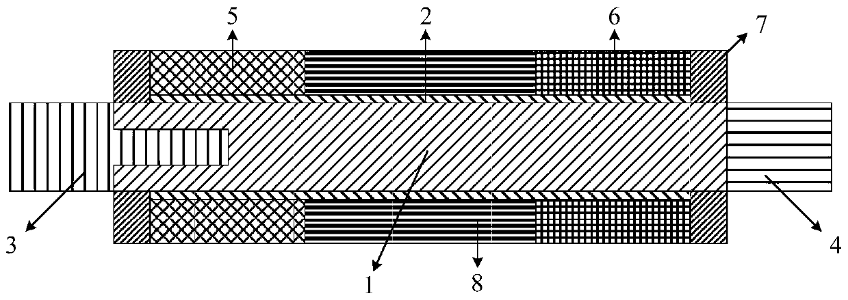
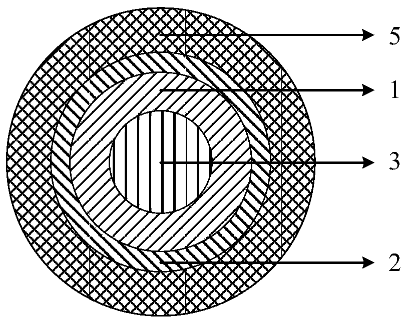
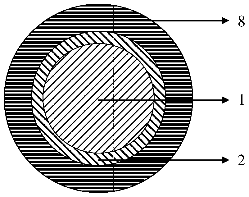
[0029] refer to Figure 1-2 , the present invention includes a nanowire channel 1, a gate oxide 2, a source 3 extending to the inside of the channel 1, a drain 4, a control gate 5, a polarity gate 6, a side wall 7 and a gate isolation 8 , in the nanowire channel 1 near one end of the control gate (Control Gate) 5, the source electrode 3 composed of metal silicide continues to extend a certain length toward the inside of the channel 1, and the diameter of the source electrode in the extension part should be less than or equal to the nanowire diameter.

[0030] An asymmetrical reconfigurable field effect transistor, which includes a drain 4 arranged at one end of the channel 1 and a source 3 extending to the inside of the channel 1 at the other end of the channel 1, and a drain 4 arranged outside the channel 1 Gate oxide 2, control gate 5 and polarity...


PUM


Abstract

The invention discloses an asymmetrical reconfigurable field effect transistor. The transistor comprises a channel, a drain arranged at one end of the channel, a source extended to the inside of the channel at the other end of the channel, and a drain arranged at one end of the channel. The gate oxide on the outside, the control gate and the polarity gate respectively arranged on the source and drain terminals and outside the gate oxide, respectively arranged outside the two ends of the channel, are used for the control gate, the polarity gate The side wall electrically isolating the source and the drain, and the gate isolation arranged outside the gate oxide for isolating the control gate and the polarity gate. In the present invention, the contact area between the source end extending into the channel and the nanowire channel is larger, thereby increasing the tunneling area of ​​carriers and increasing the turn-on current. When it is turned off, the drain structure is the same as the non-overlapping area of ​​the general RFET drain structure, and the leakage current remains basically unchanged, so the current switching ratio is improved, and the logic gate current is shortened while keeping the static power consumption unchanged. operation delay time.

Description

technical field [0001] The invention belongs to digital logic and memory devices in CMOS very large integrated circuits (VLSI), in particular to an asymmetric reconfigurable field effect transistor. Background technique [0002] The size and function scaling of CMOS devices is pushing information processing technology into new application fields. This scaling enables many applications to be realized through stronger performance and higher complexity. However, because the reduction of device size will eventually reach the physical limit in the future, new information processing devices and micro-architectures are currently being explored to continue the development cycle of integrated circuits that doubles the performance of chips with the same area every 18 months in history, and can be reconfigured Field Effect Transistor (RFET) is one of them. Because RFET is a device that can obtain N-type and P-type electrical characteristics by applying different voltages on the port, ...

Claims


Application Information

Patent Timeline
Patent Type & Authority Patents(China)
IPC IPC(8): H01L29/08H01L29/06H01L29/47H01L29/739H01L51/05H01L51/10B82Y40/00
CPCH01L29/7391H01L29/0669H01L29/0843H01L29/47B82Y40/00H10K10/46H10K10/80
Inventor 李相龙孙亚宾李小进石艳玲王昌锋廖端泉田明曹永峰
Owner EAST CHINA NORMAL UNIV
Why Eureka
Try Eureka