Data transfer between chips in a multi-chip semiconductor device with an increased data transfer speed

a data transfer speed and semiconductor technology, applied in the direction of transmission monitoring, pulse technique, instruments, etc., can solve the problems of essentially no good lamination type semiconductor device, limited number of wires, and limitations in the miniaturization of semiconductor integrated circuits, so as to prevent a reduction in the amount of data to be transferred

Active Publication Date: 2012-04-03
NEC CORP +1
View PDF2 Cites 96 Cited by
  • Summary
  • Abstract
  • Description
  • Claims
  • Application Information

AI Technical Summary

Benefits of technology

[0008]It is an object of the present invention to provide a method of transferring data between chips and a multi-chip semiconductor device which are capable of preventing a reduction in the amount of data to be transferred between chips, without increasing the total number of inter-chip wires, when a faulty inter-chip wire(s) is / are encountered.
[0009]First, a test is conducted to determine whether or not each inter-chip wire is capable of normally transferring data, on circuits arranged on chips between which the inter-chip wire is connected. When there exists an inter-chip wire incapable of normally transferring data, the data transfer speed of a buffer circuit on a chip on the transmission side which is connected to an inter-chip wire capable of normally transferring data, is increased. The buffer circuit, whose data transfer speed has been increased, transfers data to be transferred through the inter-chip wire which is incapable of normally transferring data, together with data which should originally be transferred by the buffer circuit, to a chip on the reception side through an inter-chip wire connected to the buffer circuit, at the increased data transfer speed.
[0010]Thus, the present invention makes it possible to avoid a reduction in bandwidth for data transfer between chips when there exist(s) an inter-chip wire(s) having a faulty connection in a multi-chip semiconductor device, because the speed of data transfer through another inter-chip wire is increased, and this inter-chip wire is used to transfer data which should otherwise be transferred through the inter-chip wire having a faulty connection.

Problems solved by technology

However, since miniaturization of semiconductor integrated circuits has limitations, the introduction of new technologies has been needed for further increasing the density of integration.
In these semiconductor devices, although chips are interconnected through bonding wires, the number of wires is limited to approximately one hundred.
If the number of inter-chip wires increases to several thousands due to through wiring, even 1% of faulty through wires means that there will be essentially no good lamination type semiconductor devices.
However, if the number of faulty inter-chip wires increases by several tens of percent, the total number of inter-chip wires also increases by several tens of percent due to the spare inter-chip wires.
In spite of a semiconductor device being multi-layered to increase the density of semiconductor circuits, the area occupied by the spare inter-chip wires can limit improvement in the density of semiconductor circuits.

Method used


Image

  • Data transfer between chips in a multi-chip semiconductor device with an increased data transfer speed
  • Data transfer between chips in a multi-chip semiconductor device with an increased data transfer speed
  • Data transfer between chips in a multi-chip semiconductor device with an increased data transfer speed

Examples


first exemplary embodiment

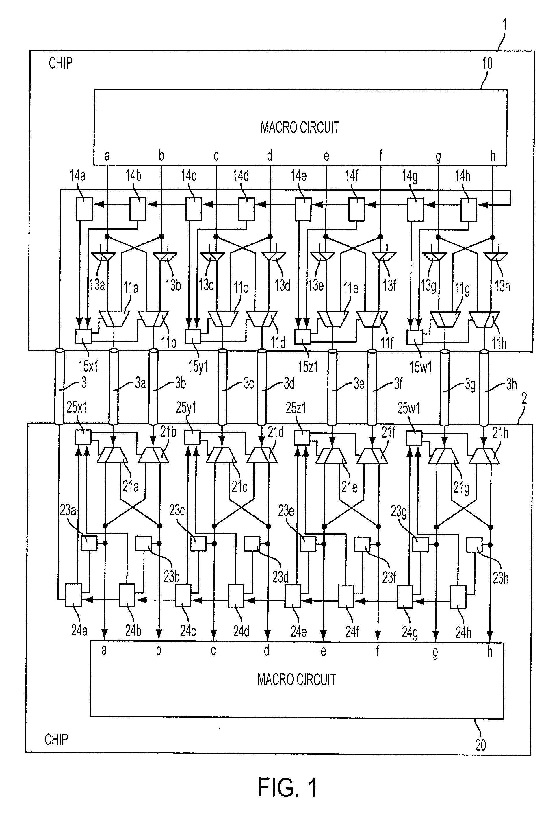
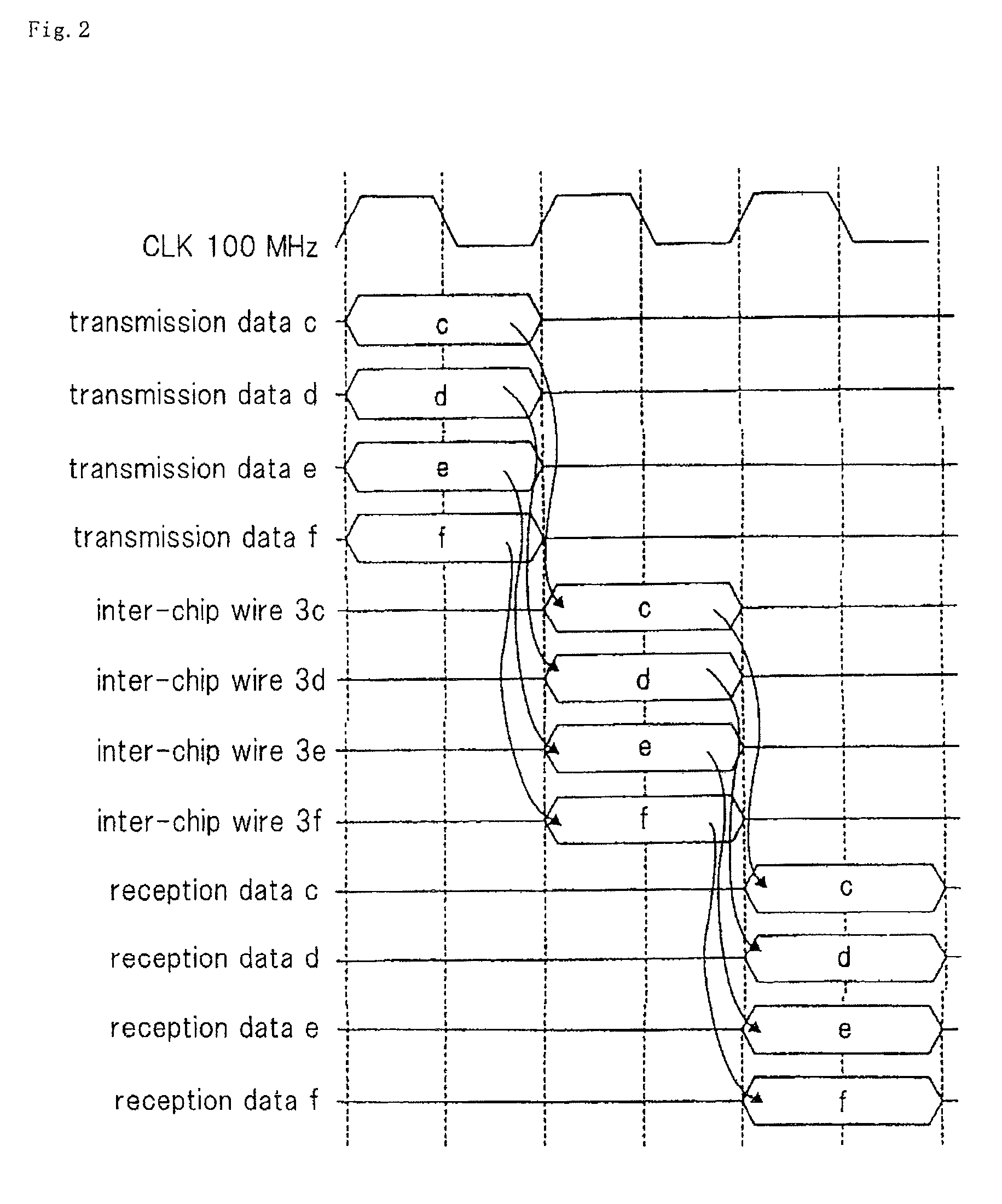
[0037]FIG. 1 is a block diagram of a multi-chip semiconductor device according to a first exemplary embodiment of the present invention. The multi-chip semiconductor device of this exemplary embodiment comprises two semiconductor chips 1, 2; 8 chip wires 3a, 3b, 3c, 3d, 3e, 3f, 3g, and 3h; and test result transmission inter-chip wire 3. In this exemplary embodiment, the clock signal used for data transfer between the chips has a frequency of 100 MHz, and therefore the bandwidth between the chips is 800 Mpbs.

[0038]Chip 1 includes macro circuit 10; transmission buffer circuits 11a 11b, 11c, 11d, 11e, 11f, 11g, and 11h; selectors 13a, 13b, 13c, 13d, 13e, 13f, 13g, and 13h, registers 14a, 14b, 14c, 14d, 14e, 14f, 14g, and 14h; and transfer speed control units 15x1, 15y1, 15z1, and 15w1. Transfer speed control units 15x1 to 15w1 make up a transfer speed control means. Macro circuit 10 outputs 8-bit data comprised of 1-bit data a, b, c, d, e, f, g, and h. Selectors 13a, 13b, 13c, 13d, 13e...

second exemplary embodiment

[0050]FIG. 6 is a block diagram of a multi-chip semiconductor device according to a second exemplary embodiment of the present invention.

[0051]In the first exemplary embodiment, in order to determine whether the connection of each inter-chip wire is good or faulty, a test signal having a certain defined test pattern is transmitted from chip 1 to chip 2, and the connection determination unit in chip 2 determines whether or not a test signal having the test pattern has been received.

[0052]In this exemplary embodiment, the data transfer speeds of transmission buffer circuits 11a, 11b connected with inter-chip wire 3a, 3b to be tested for connection are doubled, and test signal ta to be applied to selector 13a is fixed at a low level, while test signal tb to be applied to selector 13b is fixed at a high level, such that transmission buffer circuits 11a, 11b alternately transfer a test signal having a high level and a test signal having a low level to chip 2 through inter-chip wire 3a, 3...

third exemplary embodiment

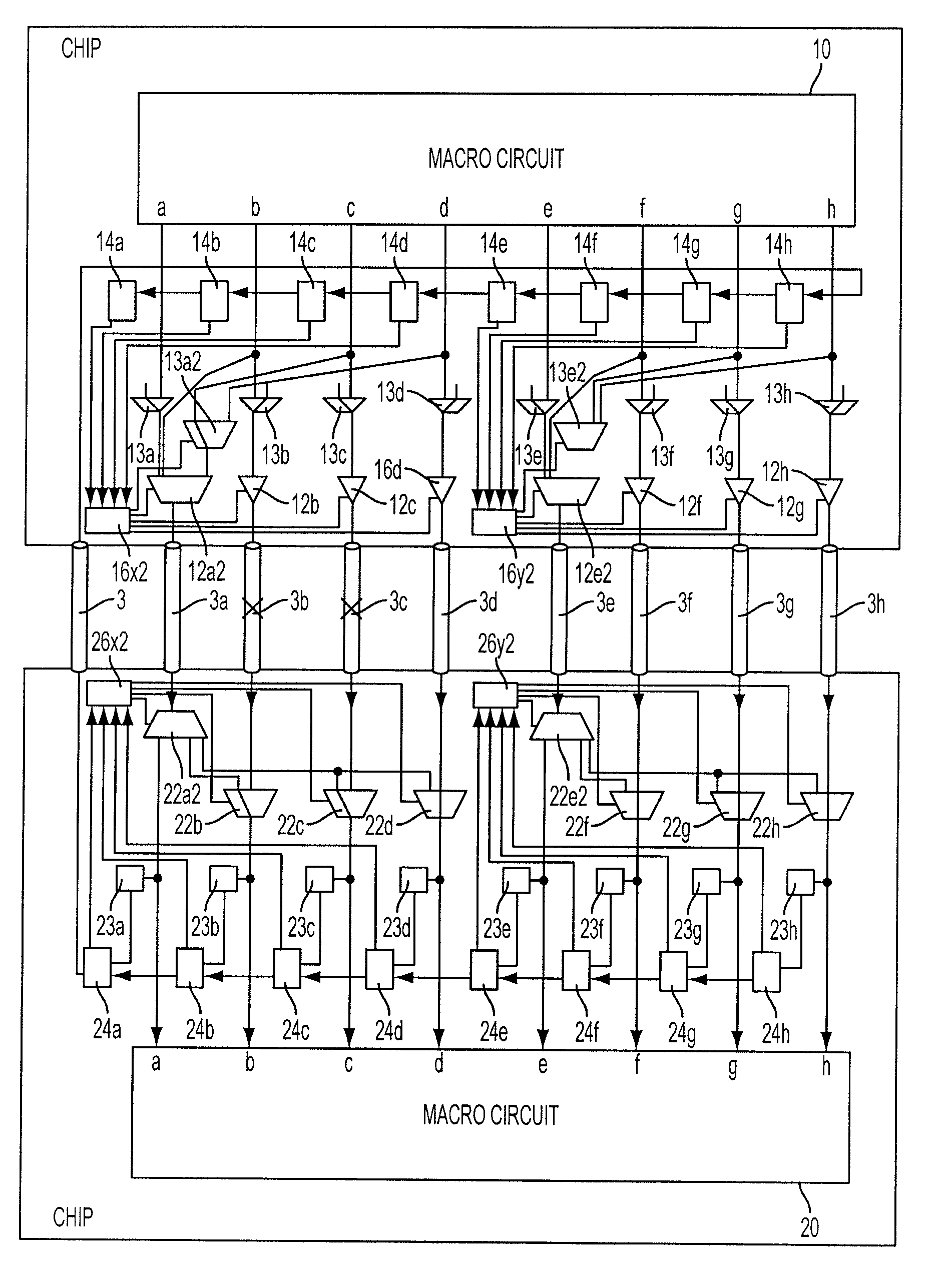
[0053]In the first exemplary embodiment, the data transfer speeds of a transmission buffer circuit connected with an inter-chip wire adjacent to an inter-chip wire having a faulty connection is doubled. However, a transmission buffer circuit whose data transfer speed is doubled is not limited to a transmission buffer circuit connected with an inter-chip wire adjacent to an inter-chip wire having a faulty connection.

[0054]In this exemplary embodiment, transmission buffer circuits whose data transfer speed can be doubled are limited to transmission buffer circuit 12a1 connected with first data transfer inter-chip wire 3a and transmission buffer circuit 12e1 connected with fifth data transfer inter-chip wire 3e. If second and seventh inter-chip wires 3b, 3g have faulty connections, data b which would otherwise be sent through second inter-chip wire 3b is transferred through first inter-chip wire 3a, and data g which would otherwise be sent through seventh inter-chip wire 3g is transfer...


PUM


Abstract

A data transfer method is disclosed in a multi-chip semiconductor device which comprises a plurality of inter-chip wires. First, a test is conducted to determine whether or not each inter-chip wire is capable of normally transferring data, on circuits arranged on chips between which the inter-chip wire is connected. When an inter-chip wire incapable of normally transferring data exists, the data transfer speed of the buffer circuit that is on the chip on the transmission and that is connected to an inter-chip wire capable of normally transferring data is increased. The buffer circuit, whose data transfer speed has been increased, transfers data which would otherwise be transferred through the inter-chip wire incapable of normally transferring data, together with the data which should be transferred thereby, to the chip on the reception side chip through an inter-chip wire connected to the buffer circuit at the data transfer speed.

Description

[0001]This application is based upon and claims the benefit of priority from Japanese patent application No. 2007-310921 filed on Nov. 30, 2007, the disclosure of which is incorporated herein in its entirety by reference.BACKGROUND OF THE INVENTION[0002]1. Field of the Invention[0003]The present invention relates to a multi-chip semiconductor device which comprises two or more semiconductor chips, and a plurality of inter-chip wires for transferring data in synchronization with a clock signal between the semiconductor chips, and more particularly, to a method of transferring data between the chips.[0004]2. Description of the Related Art[0005]Miniaturization of semiconductor integrated circuits has improved the density of integration, and promotes higher performance of CPU and larger memory capacities. However, since miniaturization of semiconductor integrated circuits has limitations, the introduction of new technologies has been needed for further increasing the density of integrat...

Claims


Application Information

Patent Timeline
Patent Type & Authority Patents(United States)
IPC IPC(8): H04B1/38G06F13/38G06F13/42G11C5/00G11C5/04H03K19/00
CPCG11C29/025H01L25/0657H01L24/49G11C5/04H01L2225/06513H01L2225/06541H01L2924/3011H01L2224/48137H01L2224/49175H01L2924/00H01L2924/00014H01L2924/14H01L24/48H01L2224/45099
Inventor SAITO, HIDEAKIIKEDA, HIROAKI
Owner NEC CORP
Why Eureka
Try Eureka