Predicting parasitic capacitance in schematic circuit simulations using sub-circuit modeling

a schematic circuit and sub-circuit technology, applied in the field of integrative circuit devices, can solve the problems of long circuit design cycle, difficult to predict circuit performance at early stages of circuit design, and significant parasitic effects once considered minor

Active Publication Date: 2012-04-03
XILINX INC
View PDF3 Cites 16 Cited by
  • Summary
  • Abstract
  • Description
  • Claims
  • Application Information

AI Technical Summary

Problems solved by technology

As IC fabrication technology continues to improve and circuit components become smaller, parasitic effects once considered minor become more significant, particularly when estimating circuit performance during simulation.
This difference in simulation resul

Method used


Image

  • Predicting parasitic capacitance in schematic circuit simulations using sub-circuit modeling
  • Predicting parasitic capacitance in schematic circuit simulations using sub-circuit modeling
  • Predicting parasitic capacitance in schematic circuit simulations using sub-circuit modeling

Examples


Embodiment Construction

[0020]While the specification concludes with claims defining the features of the invention that are regarded as novel, it is believed that the invention will be better understood from a consideration of the description in conjunction with the drawings. As required, detailed embodiments of the present invention are disclosed herein; however, it is to be understood that the disclosed embodiments are merely exemplary of the invention, which can be embodied in various forms. Therefore, specific structural and functional details disclosed herein are not to be interpreted as limiting, but merely as a basis for the claims and as a representative basis for teaching one skilled in the art to variously employ the inventive arrangements in virtually any appropriately detailed structure. Further, the terms and phrases used herein are not intended to be limiting but rather to provide an understandable description of the invention.

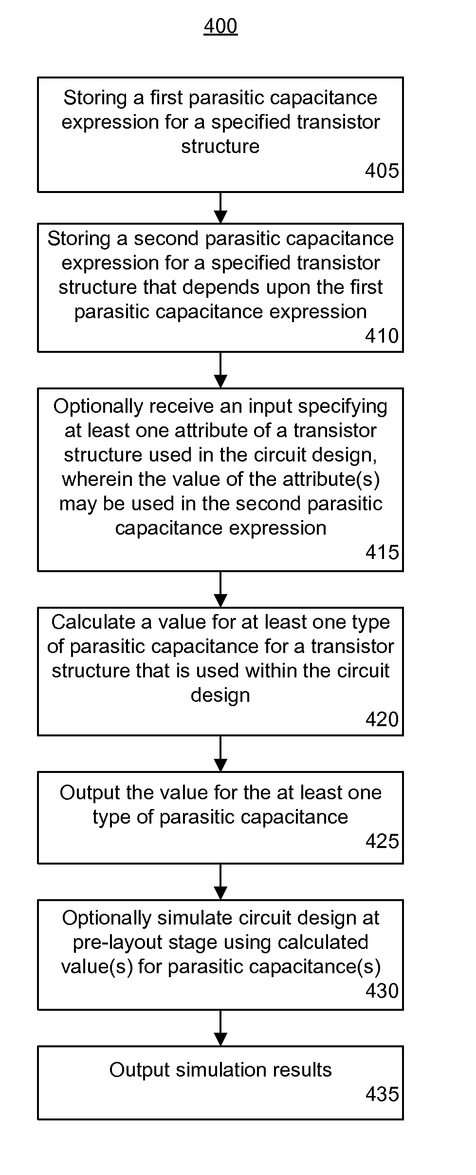
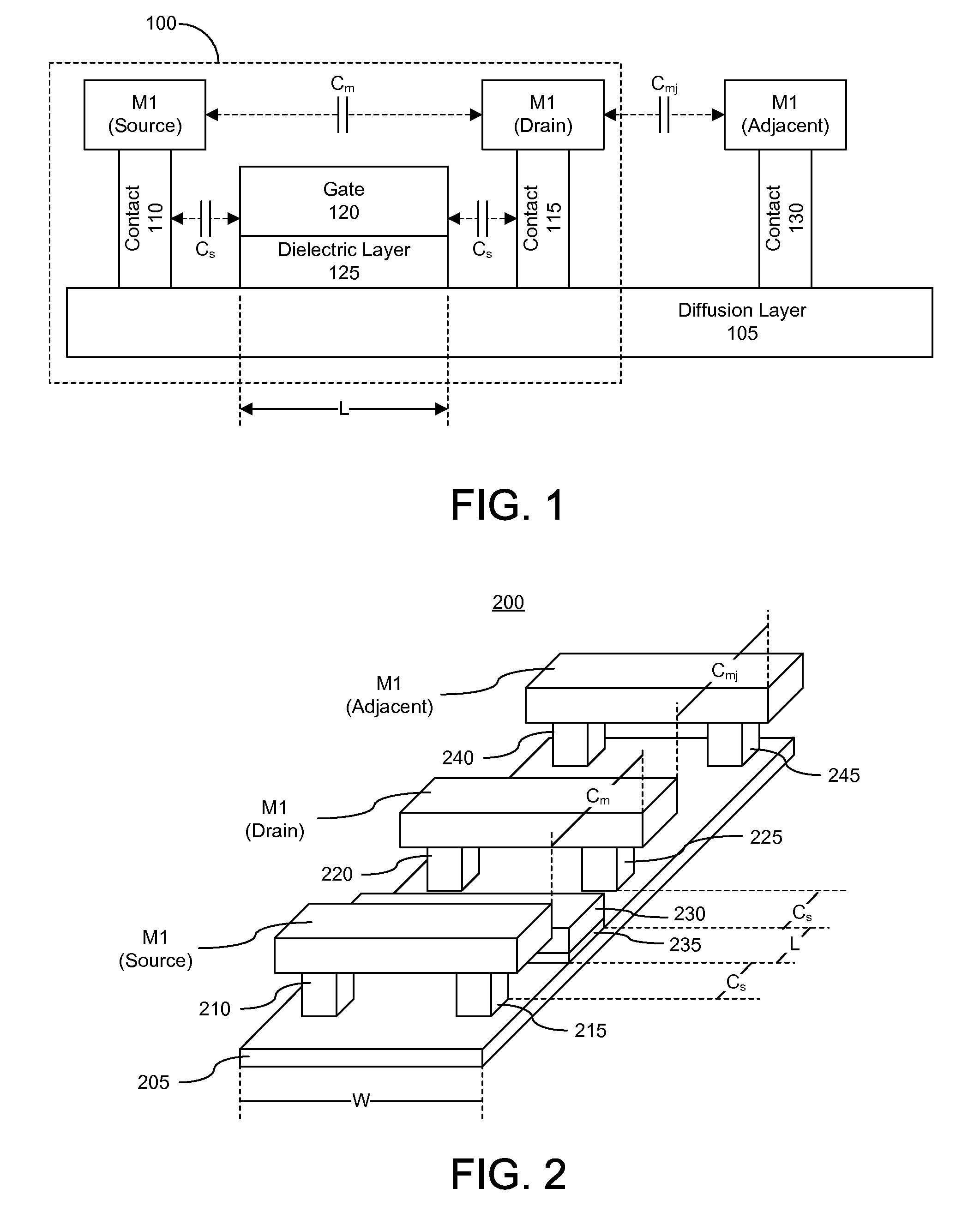
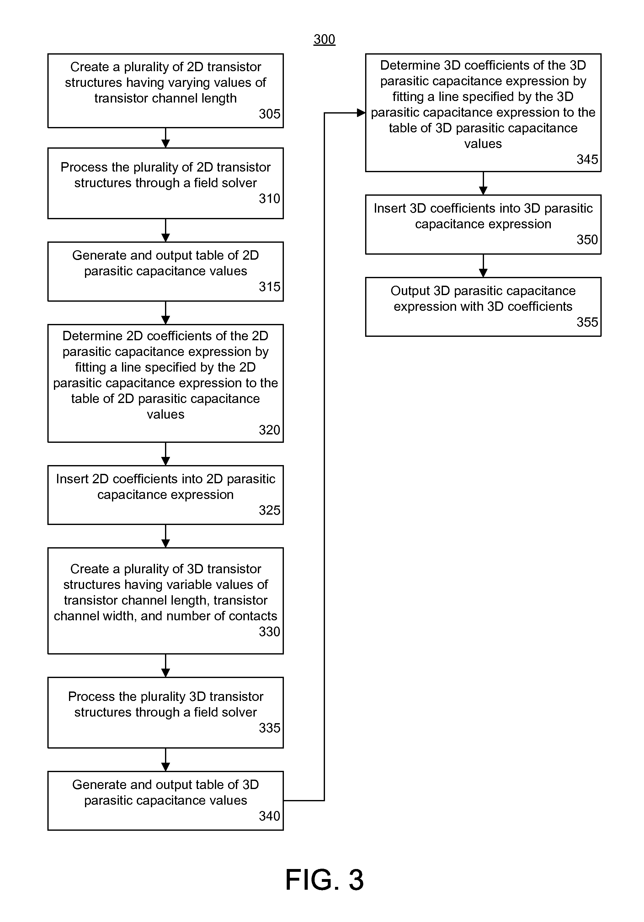
[0021]The embodiments disclosed herein relate to determining paras...


PUM


Abstract

A computer-implemented method of determining parasitic capacitance for transistors within an integrated circuit can include determining a first set of coefficients for a first expression that calculates parasitic capacitance for a transistor structure according to a first plurality of parasitic capacitances derived from a plurality of two-dimensional transistor structures (320). The first set of coefficients can be inserted into the first expression (325). The method further can include determining a second set of coefficients for a second expression that calculates parasitic capacitance for a transistor structure according to a second plurality of parasitic capacitances derived from a plurality of three-dimensional transistor structures (345). The second expression can include the first expression (350). The method can include inserting the second set of coefficients into the second expression and outputting the second expression (355).

Description

FIELD OF THE INVENTION[0001]The embodiments disclosed herein relate to integrated circuit devices (ICs). More particularly, the embodiments relate to determining parasitic capacitances in schematic circuit simulations for an IC.BACKGROUND OF THE INVENTION[0002]Simulation is invaluable when creating circuit designs for implementation within integrated circuits (ICs). Often, circuit designs are simulated at the schematic level. That is, circuit designs can be simulated prior to layout of the circuit design. This means that the circuit can be simulated with respect to functionality, timing, and other aspects purely from the schematic of the circuit design prior to determining where the various components of the circuit design will be located on the target IC.[0003]As IC fabrication technology continues to improve and circuit components become smaller, parasitic effects once considered minor become more significant, particularly when estimating circuit performance during simulation. The...

Claims


Application Information

Patent Timeline
IPC IPC(8): G06F17/10G06F17/50
CPCG06F17/5036G06F30/367
Inventor WU, SHUXIANYU, TAO
Owner XILINX INC
Why Eureka
Try Eureka