Light emitting diode with improved structure

a light-emitting diode and improved structure technology, applied in the field of non-polar light-emitting diodes, can solve the problems of pin holes, cracks or warpages in the semiconductor layer, dislocation, etc., and achieve the effect of enhancing the recombination efficiency of electrons and holes and minimizing the generation of crystal defects

Active Publication Date: 2012-04-10
SEOUL VIOSYS CO LTD
View PDF26 Cites 8 Cited by
  • Summary
  • Abstract
  • Description
  • Claims
  • Application Information

AI Technical Summary

Benefits of technology

[0015]This invention provides an LED for minimizing generation of crystal defects in an active region and enhancing recombination efficiency of electrons and holes in the active region.
[0017]The present invention discloses an LED including non-polar GaN-based semiconductor layers grown on a non-polar substrate, wherein the semiconductor layers include a non-polar N-type semiconductor layer, a non-polar P-type semiconductor layer, and active region layers positioned between the N-type and P-type semiconductor layers. In addition, the active region layers have a structure having a well layer and a barrier layer with a superlattice structure. The non-polar GaN-based semiconductor layers are used, thereby enhancing recombination efficiency of electrons and holes in an active region having the active region layers. In addition to the enhanced recombination efficiency of electrons and holes, the barrier layer with a superlattice structure is employed in the active region, thereby minimizing occurrence of defects caused by lattice mismatch between well and barrier layers.
[0021]In some embodiments, the well layer is formed of InxGa(1-x)N, and the barrier layer includes a lower superlattice having InyGa(1-y)N and GaN alternately laminated, an upper superlattice having InyGa(1-y)N and GaN alternately laminated, and a middle superlattice interposed between the lower and upper superlattices and having InzGa(1-z)N and GaN alternately laminated, where 0<x<1, 0<y<0.05, 0<z<0.1 and y<z<x. Here, a superlattice with a large In content is disposed between superlattices with a small In content. Accordingly, superlattices with different In contents are laminated, thereby reducing pin holes and hillrocks.

Problems solved by technology

However, if a Group-III-element nitride semiconductor layer is grown on the different-type substrate 11, a crack or warpage occurs in the semiconductor layer and dislocation is produced due to the difference of lattice coefficients and thermal expansion coefficients between the semiconductor layer and the substrate.
Such lattice mismatch between the layers causes pin holes, surface roughness, and degradation of crystal structures.
In addition, interface stress between different kinds of layers may additionally cause piezoelectric polarization.

Method used


Image

  • Light emitting diode with improved structure
  • Light emitting diode with improved structure
  • Light emitting diode with improved structure

Examples


Embodiment Construction

[0033]Hereinafter, embodiments of the present invention will be described in detail with reference to the accompanying drawings. The following embodiments are provided only for illustrative purposes so that those skilled in the art can fully understand the spirit of the present invention. Therefore, the present invention is not limited to the following embodiments but may be implemented in other forms. In the drawings, the widths, lengths, thicknesses and the like of elements may be exaggerated for convenience of illustration. Like reference numerals indicate like elements throughout the specification and drawings.

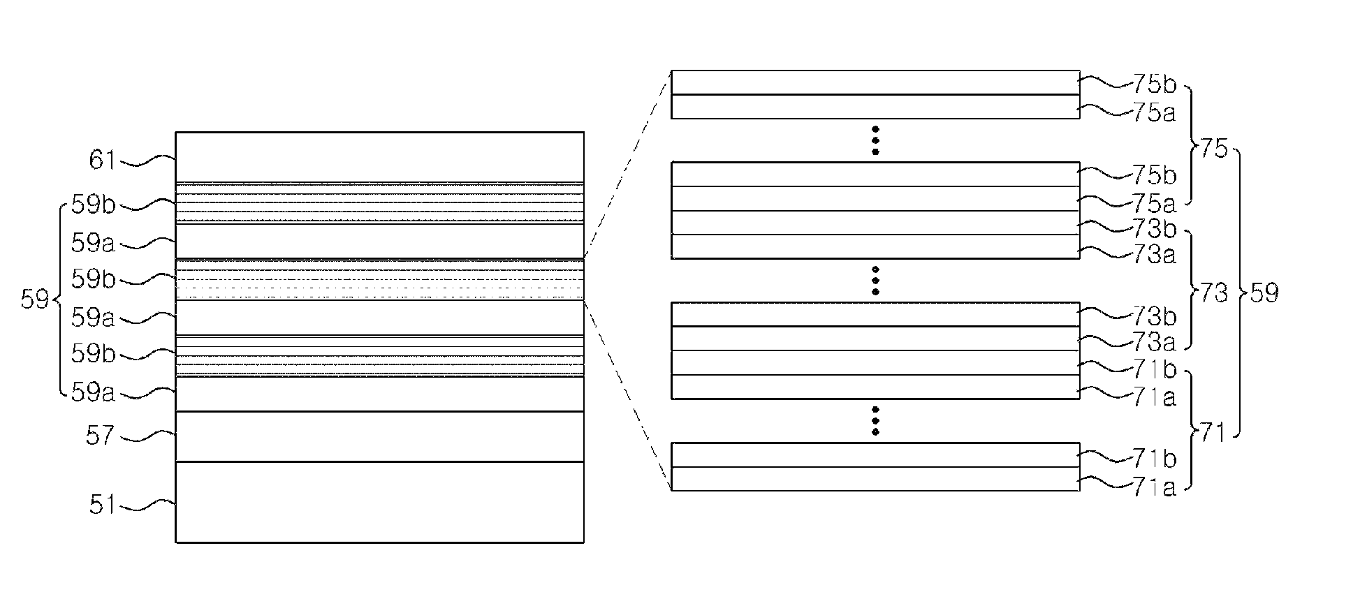
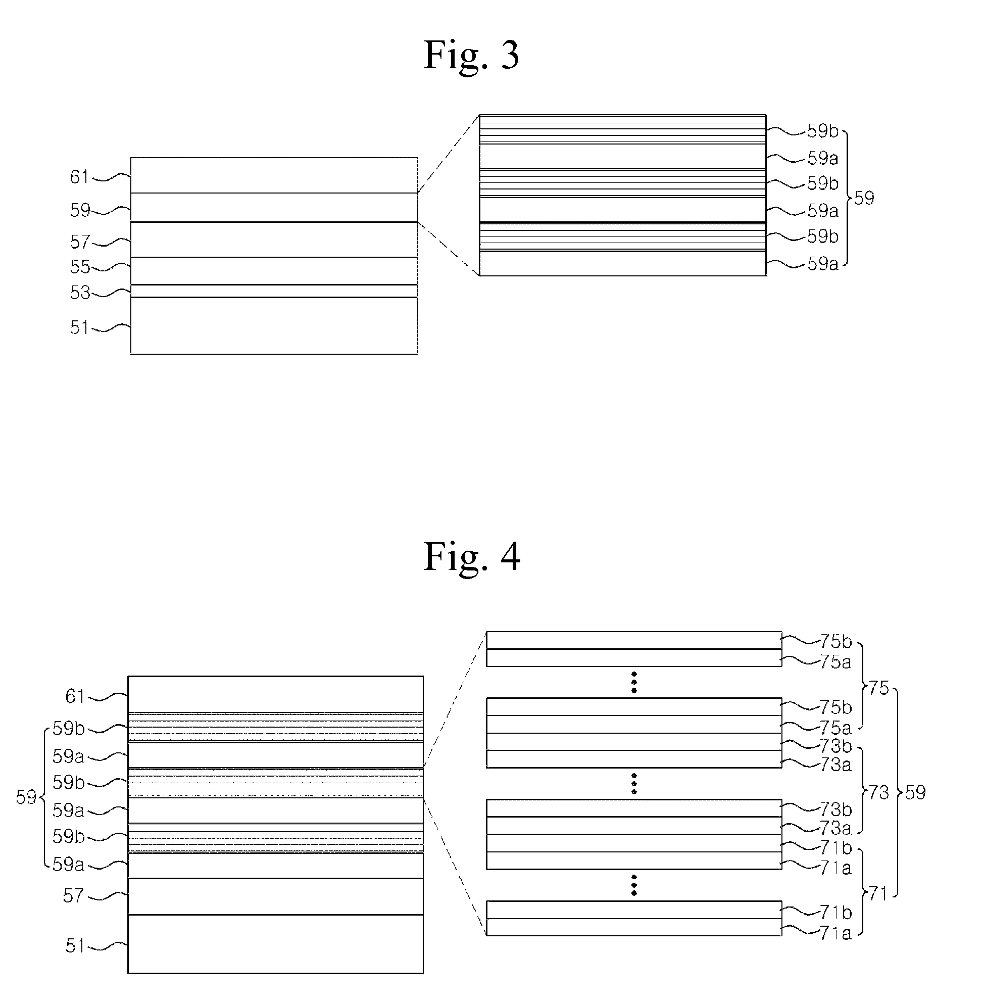
[0034]FIG. 3 is a sectional view illustrating an LED according to an embodiment of the present invention.

[0035]Referring to FIG. 3, an N-type compound semiconductor layer 57 is positioned on top of a substrate 51. Also, a buffer layer may be interposed between the substrate 51 and the N-type semiconductor layer 57, and the buffer layer may include a low-temperature buffer ...


PUM


Abstract

A light emitting diode (LED) for minimizing crystal defects in an active region and enhancing recombination efficiency of electrons and holes in the active region includes non-polar GaN-based semiconductor layers grown on a non-polar substrate. The semiconductor layers include a non-polar N-type semiconductor layer, a non-polar P-type semiconductor layer, and non-polar active region layers positioned between the N-type semiconductor layer and the P-type semiconductor layer. The non-polar active region layers include a well layer and a barrier layer with a superlattice structure.

Description

CROSS REFERENCE TO RELATED APPLICATION[0001]This application claims priority from and the benefit of Korean Patent Application No. 10-2007-0091679, filed on Sep. 10, 2007, which is hereby incorporated by reference for all purposes as if fully set forth herein.BACKGROUND OF THE INVENTION[0002]1. Field of the Invention[0003]The present invention relates to a light emitting diode formed through growth of non-polar GaN-based semiconductor layers, and more particularly, to a non-polar light emitting diode having a barrier layer with a superlattice structure.[0004]2. Discussion of the Background[0005]In general, since Group-III-element nitrides, such as GaN, AlN and InGaN, have excellent thermal stability and a direct-transition-type energy band structure, they have recently come into the spotlight as materials for light emitting diodes (LEDs) in blue and ultraviolet regions. Particularly, an InGaN compound semiconductor has been noticed for its narrow band gap. LEDs using such a GaN-base...

Claims


Application Information

Patent Timeline
Patent Type & Authority Patents(United States)
IPC IPC(8): H01L29/06
CPCH01L33/16H01L33/32H01L33/06
Inventor LEE, CHUNG HOONNAM, KI BUMKAL, DAE SUNG
Owner SEOUL VIOSYS CO LTD
Why Eureka
Try Eureka